OT-23 DBV 5 250 Green (RoHS & no Sb/Br) CU NIPDAU Level-1-260C-UNLIM SN74LVC1G32DBVTE4 ACTIVE SOT-23 DBV 5 250 Green (RoHS & no Sb/Br) CU NIPDAU Level-1-260C-UNLIM SN74LVC1G32DCKR ACTIVE SC70 DCK 5 3000 Green (RoHS & no Sb/Br) CU NIPDAU Level-1-260C-UNLIM SN74LVC1G32DCKRE4 ACTIVE SC70 DCK 5 3000 Green (RoHS & no Sb/Br) CU NIPDAU Level-1-260C-UNLIM SN74LVC1G32DCKRG4 ACTIVE SC70 DCK 5 3000 Green (RoHS & no Sb/Br) CU NIPDAU Level-1-260C-UNLIM SN74LVC1G32DCKT ACTIVE SC70 DCK 5 250 Green (RoHS & no Sb/Br) CU NIPDAU Level-1-260C-UNLIM SN74LVC1G32DCKTE4 ACTIVE SC70 DCK 5 250 Green (RoHS & no Sb/Br) CU NIPDAU Level-1-260C-UNLIM SN74LVC1G32DRLR ACTIVE SOP DRL 5 4000 Green (RoHS & no Sb/Br) CU NIPDAU Level-1-260C-UNLIM SN74LVC1G32DRLRG4 ACTIVE SOP DRL 5 4000 Green (RoHS & no Sb/Br) CU NIPDAU Level-1-260C-UNLIM SN74LVC1G32YEAR ACTIVE WCSP YEA 5 3000 TBD SNPB Level-1-260C-UNLIM SN74LVC1G32YEPR ACTIVE WCSP YEP 5 3000 TBD SNPB Level-1-260C-UNLIM SN74LVC1G32YZAR ACTIVE WCSP YZA 5 3000 Pb-Free (RoHS) SNAGCU Leve
 24 Pages, 795 KB, Original
OT-23 DBV 5 250 Green (RoHS & no Sb/Br) CU NIPDAU Level-1-260C-UNLIM SN74LVC1G32DBVTE4 ACTIVE SOT-23 DBV 5 250 Green (RoHS & no Sb/Br) CU NIPDAU Level-1-260C-UNLIM SN74LVC1G32DCKR ACTIVE SC70 DCK 5 3000 Green (RoHS & no Sb/Br) CU NIPDAU Level-1-260C-UNLIM SN74LVC1G32DCKRE4 ACTIVE SC70 DCK 5 3000 Green (RoHS & no Sb/Br) CU NIPDAU Level-1-260C-UNLIM SN74LVC1G32DCKRG4 ACTIVE SC70 DCK 5 3000 Green (RoHS & no Sb/Br) CU NIPDAU Level-1-260C-UNLIM SN74LVC1G32DCKT ACTIVE SC70 DCK 5 250 Green (RoHS & no Sb/Br) CU NIPDAU Level-1-260C-UNLIM SN74LVC1G32DCKTE4 ACTIVE SC70 DCK 5 250 Green (RoHS & no Sb/Br) CU NIPDAU Level-1-260C-UNLIM SN74LVC1G32DRLR ACTIVE SOP DRL 5 4000 Green (RoHS & no Sb/Br) CU NIPDAU Level-1-260C-UNLIM SN74LVC1G32DRLRG4 ACTIVE SOP DRL 5 4000 Green (RoHS & no Sb/Br) CU NIPDAU Level-1-260C-UNLIM SN74LVC1G32YEAR ACTIVE WCSP YEA 5 3000 TBD SNPB Level-1-260C-UNLIM SN74LVC1G32YEPR ACTIVE WCSP YEP 5 3000 TBD SNPB Level-1-260C-UNLIM SN74LVC1G32YZAR ACTIVE WCSP YZA 5 3000 Pb-Free (RoHS) SNAGCU Leve
 23 Pages, 724 KB, Original
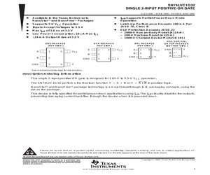
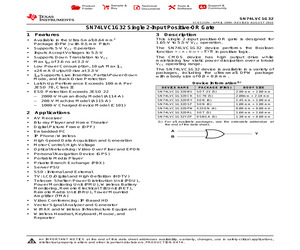
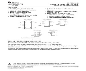
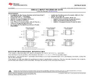
 - WCSP (DSBGA) 0.23-mm Large Bump - YZP (Pb-free) Reel of 3000 SN74LVC1G32YZPR _ _ _CG_ SON - DRY Reel of 5000 SN74LVC1G32DRYR CG_ SN74LVC1G32DBVR Reel of 3000 SOT (SOT-23) - DBV SN74LVC1G32DBVRG4 Tube of 250 -40C to 85C SOT (SC-70) - DCK SN74LVC1G32DBVT SN74LVC1G32DCKRE4 SN74LVC1G32DCKRG4 Tube of 250 SOT (SOT-553) - DRL (2) Reel of 4000 CG_ SN74LVC1G32DCKT SN74LVC1G32DCKTE4 SN74LVC1G32DRLR SN74LVC1G32DRLRG4 CG_ Package drawings, standard packing quantities, thermal data, symbolization, and PCB design guidelines are available at www.ti.com/sc/package. DBV/DCK/DRL/DRY: The actual top-side marking has one additional character that designates the assembly/test site. YZP: The actual top-side marking has three preceding characters to denote year, month, and sequence code, and one following character to designate the assembly/test site. Pin 1 identifier indicates solder-bump composition (1 = SnPb, * = Pb-free). FUNCTION TABLE INPUTS B OUTPUT Y H X H X H H L L L A LOGIC DIAGRAM (POSITIVE LOGIC) 2 C32_
 18 Pages, 730 KB, Original
 - WCSP (DSBGA) 0.23-mm Large Bump - YZP (Pb-free) Reel of 3000 SN74LVC1G32YZPR _ _ _CG_ SON - DRY Reel of 5000 SN74LVC1G32DRYR CG_ SN74LVC1G32DBVR Reel of 3000 SOT (SOT-23) - DBV SN74LVC1G32DBVRG4 Tube of 250 -40C to 85C SOT (SC-70) - DCK SN74LVC1G32DBVT SN74LVC1G32DCKRE4 SN74LVC1G32DCKRG4 Tube of 250 SOT (SOT-553) - DRL (2) Reel of 4000 CG_ SN74LVC1G32DCKT SN74LVC1G32DCKTE4 SN74LVC1G32DRLR SN74LVC1G32DRLRG4 CG_ Package drawings, standard packing quantities, thermal data, symbolization, and PCB design guidelines are available at www.ti.com/sc/package. DBV/DCK/DRL/DRY: The actual top-side marking has one additional character that designates the assembly/test site. YZP: The actual top-side marking has three preceding characters to denote year, month, and sequence code, and one following character to designate the assembly/test site. Pin 1 identifier indicates solder-bump composition (1 = SnPb, * = Pb-free). FUNCTION TABLE INPUTS B OUTPUT Y H X H X H H L L L A LOGIC DIAGRAM (POSITIVE LOGIC) 2 C32_
 17 Pages, 621 KB, Original
00 SN74LVC1G32DRYR CG SN74LVC1G32DBVR Reel of 3000 SOT (SOT-23) - DBV SN74LVC1G32DBVRE4 SN74LVC1G32DBVRG4 Tube of 250 -40C to 85C C32_ SN74LVC1G32DBVT SN74LVC1G32DCKR Reel of 3000 SOT (SC-70) - DCK SN74LVC1G32DCKRG4 Tube of 250 SOT (SOT-553) - DRL (1) (2) SN74LVC1G32DCKRE4 Reel of 4000 CG_ SN74LVC1G32DCKT SN74LVC1G32DCKTE4 SN74LVC1G32DRLR SN74LVC1G32DRLRG4 CG_ Package drawings, standard packing quantities, thermal data, symbolization, and PCB design guidelines are available at www.ti.com/sc/package. DBV/DCK/DRL: The actual top-side marking has one additional character that designates the assembly/test site. YZP: The actual top-side marking has three preceding characters to denote year, month, and sequence code, and one following character to designate the assembly/test site. Pin 1 identifier indicates solder-bump composition (1 = SnPb, * = Pb-free). Table 1. FUNCTION TABLE INPUTS B OUTPUT Y H X H X H H L L L A LOGIC DIAGRAM (POSITIVE LOGIC) 2 Submit Documentation Feedback Copyright (c) 1999-2011,
 25 Pages, 1023 KB, Original
00 SN74LVC1G32DRYR CG SN74LVC1G32DBVR Reel of 3000 SOT (SOT-23) - DBV SN74LVC1G32DBVRE4 SN74LVC1G32DBVRG4 Tube of 250 -40C to 85C C32_ SN74LVC1G32DBVT SN74LVC1G32DCKR Reel of 3000 SOT (SC-70) - DCK SN74LVC1G32DCKRG4 Tube of 250 SOT (SOT-553) - DRL (1) (2) SN74LVC1G32DCKRE4 Reel of 4000 CG_ SN74LVC1G32DCKT SN74LVC1G32DCKTE4 SN74LVC1G32DRLR SN74LVC1G32DRLRG4 CG_ Package drawings, standard packing quantities, thermal data, symbolization, and PCB design guidelines are available at www.ti.com/sc/package. DBV/DCK/DRL: The actual top-side marking has one additional character that designates the assembly/test site. YZP: The actual top-side marking has three preceding characters to denote year, month, and sequence code, and one following character to designate the assembly/test site. Pin 1 identifier indicates solder-bump composition (1 = SnPb, * = Pb-free). Table 1. FUNCTION TABLE INPUTS B OUTPUT Y H X H X H H L L L A LOGIC DIAGRAM (POSITIVE LOGIC) 2 Submit Documentation Feedback Copyright (c) 1999-2011,
 24 Pages, 1085 KB, Original
LVC1G32DBVTG4 ACTIVE SOT-23 DBV 5 250 Green (RoHS & no Sb/Br) CU NIPDAU Level-1-260C-UNLIM -40 to 125 C32F SN74LVC1G32DCKR ACTIVE SC70 DCK 5 3000 Green (RoHS & no Sb/Br) CU NIPDAU | CU SN Level-1-260C-UNLIM -40 to 125 (CG5, CGF, CGK, CG R) (CGH, CGP, CGS) SN74LVC1G32DCKRE4 ACTIVE SC70 DCK 5 3000 Green (RoHS & no Sb/Br) CU NIPDAU Level-1-260C-UNLIM -40 to 125 (CG5, CGF, CGK, CG R) (CGH, CGP, CGS) SN74LVC1G32DCKRG4 ACTIVE SC70 DCK 5 3000 Green (RoHS & no Sb/Br) CU NIPDAU Level-1-260C-UNLIM -40 to 125 (CG5, CGF, CGK, CG R) (CGH, CGP, CGS) SN74LVC1G32DCKT ACTIVE SC70 DCK 5 250 Green (RoHS & no Sb/Br) CU NIPDAU | CU SN Level-1-260C-UNLIM -40 to 125 (CG5, CGF, CGK, CG R) (CGH, CGP, CGS) SN74LVC1G32DCKTG4 ACTIVE SC70 DCK 5 250 Green (RoHS & no Sb/Br) CU NIPDAU Level-1-260C-UNLIM -40 to 125 (CG5, CGF, CGK, CG R) (CGH, CGP, CGS) SN74LVC1G32DPWR ACTIVE X2SON DPW 5 3000 Green (RoHS & no Sb/Br) CU NIPDAU Level-1-260C-UNLIM -40 to 125 N4 SN74LVC1G32DRLR ACTIVE SOT-5X3 DRL 5 4000 Green (RoHS & no Sb/Br) CU NIP
 50 Pages, 2960 KB, Original
 - WCSP (DSBGA) 0.23-mm Large Bump - YZP (Pb-free) Reel of 3000 SN74LVC1G32YZPR _ _ _CG_ SON - DRY Reel of 5000 SN74LVC1G32DRYR CG_ SN74LVC1G32DBVR Reel of 3000 SOT (SOT-23) - DBV SN74LVC1G32DBVRG4 Tube of 250 -40C to 85C SOT (SC-70) - DCK SN74LVC1G32DBVT SN74LVC1G32DCKRE4 SN74LVC1G32DCKRG4 Tube of 250 SOT (SOT-553) - DRL (2) Reel of 4000 CG_ SN74LVC1G32DCKT SN74LVC1G32DCKTE4 SN74LVC1G32DRLR SN74LVC1G32DRLRG4 CG_ Package drawings, standard packing quantities, thermal data, symbolization, and PCB design guidelines are available at www.ti.com/sc/package. DBV/DCK/DRL/DRY: The actual top-side marking has one additional character that designates the assembly/test site. YZP: The actual top-side marking has three preceding characters to denote year, month, and sequence code, and one following character to designate the assembly/test site. Pin 1 identifier indicates solder-bump composition (1 = SnPb, * = Pb-free). FUNCTION TABLE INPUTS B OUTPUT Y H X H X H H L L L A LOGIC DIAGRAM (POSITIVE LOGIC) 2 C32_
 17 Pages, 621 KB, Original
 - WCSP (DSBGA) 0.23-mm Large Bump - YZP (Pb-free) Reel of 3000 SN74LVC1G32YZPR _ _ _CG_ SON - DRY Reel of 5000 SN74LVC1G32DRYR CG_ SN74LVC1G32DBVR Reel of 3000 SOT (SOT-23) - DBV SN74LVC1G32DBVRG4 Tube of 250 -40C to 85C SOT (SC-70) - DCK SN74LVC1G32DBVT SN74LVC1G32DCKRE4 SN74LVC1G32DCKRG4 Tube of 250 SOT (SOT-553) - DRL (2) Reel of 4000 CG_ SN74LVC1G32DCKT SN74LVC1G32DCKTE4 SN74LVC1G32DRLR SN74LVC1G32DRLRG4 CG_ Package drawings, standard packing quantities, thermal data, symbolization, and PCB design guidelines are available at www.ti.com/sc/package. DBV/DCK/DRL/DRY: The actual top-side marking has one additional character that designates the assembly/test site. YZP: The actual top-side marking has three preceding characters to denote year, month, and sequence code, and one following character to designate the assembly/test site. Pin 1 identifier indicates solder-bump composition (1 = SnPb, * = Pb-free). FUNCTION TABLE INPUTS B OUTPUT Y H X H X H H L L L A LOGIC DIAGRAM (POSITIVE LOGIC) 2 C32_
 17 Pages, 604 KB, Original
00 SN74LVC1G32DRYR CG SN74LVC1G32DBVR Reel of 3000 SOT (SOT-23) - DBV SN74LVC1G32DBVRE4 SN74LVC1G32DBVRG4 Tube of 250 -40C to 85C C32_ SN74LVC1G32DBVT SN74LVC1G32DCKR Reel of 3000 SOT (SC-70) - DCK SN74LVC1G32DCKRG4 Tube of 250 SOT (SOT-553) - DRL (1) (2) SN74LVC1G32DCKRE4 Reel of 4000 CG_ SN74LVC1G32DCKT SN74LVC1G32DCKTE4 SN74LVC1G32DRLR SN74LVC1G32DRLRG4 CG_ Package drawings, standard packing quantities, thermal data, symbolization, and PCB design guidelines are available at www.ti.com/sc/package. DBV/DCK/DRL: The actual top-side marking has one additional character that designates the assembly/test site. YZP: The actual top-side marking has three preceding characters to denote year, month, and sequence code, and one following character to designate the assembly/test site. Pin 1 identifier indicates solder-bump composition (1 = SnPb, * = Pb-free). Table 1. FUNCTION TABLE INPUTS B OUTPUT Y H X H X H H L L L A LOGIC DIAGRAM (POSITIVE LOGIC) 2 Submit Documentation Feedback Copyright (c) 1999-2011,
 22 Pages, 945 KB, Original
 - WCSP (DSBGA) 0.23-mm Large Bump - YZP (Pb-free) Reel of 3000 SN74LVC1G32YZPR _ _ _CG_ SON - DRY Reel of 5000 SN74LVC1G32DRYR CG_ SN74LVC1G32DBVR Reel of 3000 SOT (SOT-23) - DBV SN74LVC1G32DBVRG4 Tube of 250 -40C to 85C SOT (SC-70) - DCK SN74LVC1G32DBVT SN74LVC1G32DCKRE4 SN74LVC1G32DCKRG4 Tube of 250 SOT (SOT-553) - DRL (2) Reel of 4000 CG_ SN74LVC1G32DCKT SN74LVC1G32DCKTE4 SN74LVC1G32DRLR SN74LVC1G32DRLRG4 CG_ Package drawings, standard packing quantities, thermal data, symbolization, and PCB design guidelines are available at www.ti.com/sc/package. DBV/DCK/DRL/DRY: The actual top-side marking has one additional character that designates the assembly/test site. YZP: The actual top-side marking has three preceding characters to denote year, month, and sequence code, and one following character to designate the assembly/test site. Pin 1 identifier indicates solder-bump composition (1 = SnPb, * = Pb-free). FUNCTION TABLE INPUTS B OUTPUT Y H X H X H H L L L A LOGIC DIAGRAM (POSITIVE LOGIC) 2 C32_
 18 Pages, 488 KB, Original
 - WCSP (DSBGA) 0.23-mm Large Bump - YZP (Pb-free) Reel of 3000 SN74LVC1G32YZPR _ _ _CG_ SON - DRY Reel of 5000 SN74LVC1G32DRYR CG_ SN74LVC1G32DBVR Reel of 3000 SOT (SOT-23) - DBV SN74LVC1G32DBVRG4 Tube of 250 -40C to 85C SOT (SC-70) - DCK SN74LVC1G32DBVT SN74LVC1G32DCKRE4 SN74LVC1G32DCKRG4 Tube of 250 SOT (SOT-553) - DRL (2) Reel of 4000 CG_ SN74LVC1G32DCKT SN74LVC1G32DCKTE4 SN74LVC1G32DRLR SN74LVC1G32DRLRG4 CG_ Package drawings, standard packing quantities, thermal data, symbolization, and PCB design guidelines are available at www.ti.com/sc/package. DBV/DCK/DRL/DRY: The actual top-side marking has one additional character that designates the assembly/test site. YZP: The actual top-side marking has three preceding characters to denote year, month, and sequence code, and one following character to designate the assembly/test site. Pin 1 identifier indicates solder-bump composition (1 = SnPb, * = Pb-free). FUNCTION TABLE INPUTS B OUTPUT Y H X H X H H L L L A LOGIC DIAGRAM (POSITIVE LOGIC) 2 C32_
 17 Pages, 604 KB, Original
00 SN74LVC1G32DRYR CG SN74LVC1G32DBVR Reel of 3000 SOT (SOT-23) - DBV SN74LVC1G32DBVRE4 SN74LVC1G32DBVRG4 Tube of 250 -40C to 85C C32_ SN74LVC1G32DBVT SN74LVC1G32DCKR Reel of 3000 SOT (SC-70) - DCK SN74LVC1G32DCKRG4 Tube of 250 SOT (SOT-553) - DRL (1) (2) SN74LVC1G32DCKRE4 Reel of 4000 CG_ SN74LVC1G32DCKT SN74LVC1G32DCKTE4 SN74LVC1G32DRLR SN74LVC1G32DRLRG4 CG_ Package drawings, standard packing quantities, thermal data, symbolization, and PCB design guidelines are available at www.ti.com/sc/package. DBV/DCK/DRL: The actual top-side marking has one additional character that designates the assembly/test site. YZP: The actual top-side marking has three preceding characters to denote year, month, and sequence code, and one following character to designate the assembly/test site. Pin 1 identifier indicates solder-bump composition (1 = SnPb, * = Pb-free). Table 1. FUNCTION TABLE INPUTS B OUTPUT Y H X H X H H L L L A LOGIC DIAGRAM (POSITIVE LOGIC) 2 Submit Documentation Feedback Copyright (c) 1999-2011,
 23 Pages, 1010 KB, Original
00 SN74LVC1G32DRYR CG SN74LVC1G32DBVR Reel of 3000 SOT (SOT-23) - DBV SN74LVC1G32DBVRE4 SN74LVC1G32DBVRG4 Tube of 250 -40C to 85C C32_ SN74LVC1G32DBVT SN74LVC1G32DCKR Reel of 3000 SOT (SC-70) - DCK SN74LVC1G32DCKRG4 Tube of 250 SOT (SOT-553) - DRL (1) (2) SN74LVC1G32DCKRE4 Reel of 4000 CG_ SN74LVC1G32DCKT SN74LVC1G32DCKTE4 SN74LVC1G32DRLR SN74LVC1G32DRLRG4 CG_ Package drawings, standard packing quantities, thermal data, symbolization, and PCB design guidelines are available at www.ti.com/sc/package. DBV/DCK/DRL: The actual top-side marking has one additional character that designates the assembly/test site. YZP: The actual top-side marking has three preceding characters to denote year, month, and sequence code, and one following character to designate the assembly/test site. Pin 1 identifier indicates solder-bump composition (1 = SnPb, * = Pb-free). Table 1. FUNCTION TABLE INPUTS B OUTPUT Y H X H X H H L L L A LOGIC DIAGRAM (POSITIVE LOGIC) 2 Submit Documentation Feedback Copyright (c) 1999-2011,
 24 Pages, 1089 KB, Original
00 SN74LVC1G32DRYR CG SN74LVC1G32DBVR Reel of 3000 SOT (SOT-23) - DBV SN74LVC1G32DBVRE4 SN74LVC1G32DBVRG4 Tube of 250 -40C to 85C C32_ SN74LVC1G32DBVT SN74LVC1G32DCKR Reel of 3000 SOT (SC-70) - DCK SN74LVC1G32DCKRG4 Tube of 250 SOT (SOT-553) - DRL (1) (2) SN74LVC1G32DCKRE4 Reel of 4000 CG_ SN74LVC1G32DCKT SN74LVC1G32DCKTE4 SN74LVC1G32DRLR SN74LVC1G32DRLRG4 CG_ Package drawings, standard packing quantities, thermal data, symbolization, and PCB design guidelines are available at www.ti.com/sc/package. DBV/DCK/DRL: The actual top-side marking has one additional character that designates the assembly/test site. YZP: The actual top-side marking has three preceding characters to denote year, month, and sequence code, and one following character to designate the assembly/test site. Pin 1 identifier indicates solder-bump composition (1 = SnPb, * = Pb-free). Table 1. FUNCTION TABLE INPUTS B OUTPUT Y H X H X H H L L L A LOGIC DIAGRAM (POSITIVE LOGIC) 2 Submit Documentation Feedback Copyright (c) 1999-2011,
 23 Pages, 1014 KB, Original


