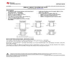
ree) Reel of 3000 SN74LVC1G32YZPR _ _ _CG_ SON - DSF Reel of 5000 SN74LVC1G32DSFR CG SON - DRY Reel of 5000 SN74LVC1G32DRYR CG SN74LVC1G32DBVR Reel of 3000 SOT (SOT-23) - DBV SN74LVC1G32DBVRE4 SN74LVC1G32DBVRG4 Tube of 250 -40C to 85C C32_ SN74LVC1G32DBVT SN74LVC1G32DCKR Reel of 3000 SOT (SC-70) - DCK SN74LVC1G32DCKRG4 Tube of 250 SOT (SOT-553) - DRL (1) (2) SN74LVC1G32DCKRE4 Reel of 4000 CG_ SN74LVC1G32DCKT SN74LVC1G32DCKTE4 SN74LVC1G32DRLR SN74LVC1G32DRLRG4 CG_ Package drawings, standard packing quantities, thermal data, symbolization, and PCB design guidelines are available at www.ti.com/sc/package. DBV/DCK/DRL: The actual top-side marking has one additional character that designates the assembly/test site. YZP: The actual top-side marking has three preceding characters to denote year, month, and sequence code, and one following character to designate the assembly/test site. Pin 1 identifier indicates solder-bump composition (1 = SnPb, * = Pb-free). Table 1. FUNCTION
 24 Pages, 1085 KB, Original
 1G32 NC7ST32M5X SN74AHCT1G32DBVR 5 1G32 NC7ST32P5 SN74AHCT1G32DCKR 5 NC7ST32P5X NC7SZ32L6X NC7SZ32M5 NC7SZ32M5X NC7SZ32P5 NC7SZ32P5X NC7SB3257P6X NC7SZ332P6 NC7SZ332P6X NC7SZ373P6 NC7SZ373P6X SN74AHCT1G32DCKR Not available SN74LVC1G32DBVR SN74LVC1G32DBVR SN74LVC1G32DCKR SN74LVC1G32DCKR Not available Not available Not available Not available Not available 5 6 5 5 5 5 6 6 6 6 6 1G32 1G32 1G32 1G32 1G32 1G32 1G3257 1G332 1G332 1G373 1G373 Fairchild Comments Specs. similar to HC Not available in tubes, use DCKR Faster, slightly lower max Vcc, not available in tubes, use DBVR Faster, slightly lower max Vcc This package Not available in tubes, use DBVR Specs. similar to HC Specs. similar to HC Not available in tubes, use DCKR Faster, slightly lower max Vcc, not available in tubes, use DBVR Faster, slightly lower max Vcc This package Not available in tubes, use DBVR Specs. similar to HC Specs. similar to HC Not available in tubes, use DCKR This package Faster, slightly lower max Vcc, not a
 329 Pages, 2106 KB, Original
 - WCSP (DSBGA) 0.23-mm Large Bump - YZP (Pb-free) Reel of 3000 SN74LVC1G32YZPR _ _ _CG_ SON - DRY Reel of 5000 SN74LVC1G32DRYR CG_ SN74LVC1G32DBVR Reel of 3000 SOT (SOT-23) - DBV SN74LVC1G32DBVRG4 Tube of 250 -40C to 85C SOT (SC-70) - DCK SN74LVC1G32DBVT SN74LVC1G32DCKRE4 SN74LVC1G32DCKRG4 Tube of 250 SOT (SOT-553) - DRL (2) Reel of 4000 CG_ SN74LVC1G32DCKT SN74LVC1G32DCKTE4 SN74LVC1G32DRLR SN74LVC1G32DRLRG4 CG_ Package drawings, standard packing quantities, thermal data, symbolization, and PCB design guidelines are available at www.ti.com/sc/package. DBV/DCK/DRL/DRY: The actual top-side marking has one additional character that designates the assembly/test site. YZP: The actual top-side marking has three preceding characters to denote year, month, and sequence code, and one following character to designate the assembly/test site. Pin 1 identifier indicates solder-bump composition (1 = SnPb, * = Pb-free). FUNCTION TABLE INPUTS B OUTPUT Y H X H X H H L L L A LOGIC DIAGRAM (POSITIVE L
 17 Pages, 621 KB, Original
 - WCSP (DSBGA) 0.23-mm Large Bump - YZP (Pb-free) Reel of 3000 SN74LVC1G32YZPR _ _ _CG_ SON - DRY Reel of 5000 SN74LVC1G32DRYR CG_ SN74LVC1G32DBVR Reel of 3000 SOT (SOT-23) - DBV SN74LVC1G32DBVRG4 Tube of 250 -40C to 85C SOT (SC-70) - DCK SN74LVC1G32DBVT SN74LVC1G32DCKRE4 SN74LVC1G32DCKRG4 Tube of 250 SOT (SOT-553) - DRL (2) Reel of 4000 CG_ SN74LVC1G32DCKT SN74LVC1G32DCKTE4 SN74LVC1G32DRLR SN74LVC1G32DRLRG4 CG_ Package drawings, standard packing quantities, thermal data, symbolization, and PCB design guidelines are available at www.ti.com/sc/package. DBV/DCK/DRL/DRY: The actual top-side marking has one additional character that designates the assembly/test site. YZP: The actual top-side marking has three preceding characters to denote year, month, and sequence code, and one following character to designate the assembly/test site. Pin 1 identifier indicates solder-bump composition (1 = SnPb, * = Pb-free). FUNCTION TABLE INPUTS B OUTPUT Y H X H X H H L L L A LOGIC DIAGRAM (POSITIVE L
 17 Pages, 604 KB, Original
ree) Reel of 3000 SN74LVC1G32YZPR _ _ _CG_ SON - DSF Reel of 5000 SN74LVC1G32DSFR CG SON - DRY Reel of 5000 SN74LVC1G32DRYR CG SN74LVC1G32DBVR Reel of 3000 SOT (SOT-23) - DBV SN74LVC1G32DBVRE4 SN74LVC1G32DBVRG4 Tube of 250 -40C to 85C C32_ SN74LVC1G32DBVT SN74LVC1G32DCKR Reel of 3000 SOT (SC-70) - DCK SN74LVC1G32DCKRG4 Tube of 250 SOT (SOT-553) - DRL (1) (2) SN74LVC1G32DCKRE4 Reel of 4000 CG_ SN74LVC1G32DCKT SN74LVC1G32DCKTE4 SN74LVC1G32DRLR SN74LVC1G32DRLRG4 CG_ Package drawings, standard packing quantities, thermal data, symbolization, and PCB design guidelines are available at www.ti.com/sc/package. DBV/DCK/DRL: The actual top-side marking has one additional character that designates the assembly/test site. YZP: The actual top-side marking has three preceding characters to denote year, month, and sequence code, and one following character to designate the assembly/test site. Pin 1 identifier indicates solder-bump composition (1 = SnPb, * = Pb-free). Table 1. FUNCTION
 25 Pages, 1023 KB, Original
-40C to 85C TOP-SIDE MARKING _ _ _CG_ SN74LVC1G32YEPR NanoFree - WCSP (DSBGA) 0.23-mm Large Bump - YZP (Pb-free) SOT (SOT-23) - DBV SOT (SC-70) - DCK SOT (SOT-553) - DRL SN74LVC1G32YZPR Reel of 3000 SN74LVC1G32DBVR Reel of 250 SN74LVC1G32DBVT Reel of 3000 SN74LVC1G32DCKR Reel of 250 SN74LVC1G32DCKT Reel of 4000 SN74LVC1G32DRLR C32_ CG_ Package drawings, standard packing quantities, thermal data, symbolization, and PCB design guidelines are available at www.ti.com/sc/package. DBV/DCK: The actual top-side marking has one additional character that designates the assembly/test site. YEA/YZA, YEP/YZP: The actual top-side marking has three preceding characters to denote year, month, and sequence code, and one following character to designate the assembly/test site. Pin 1 identifier indicates solder-bump composition (1 = SnPb, * = Pb-free). FUNCTION TABLE INPUTS A B OUTPUT Y H X H X H H L L L logic diagram (positive logic) A B 2 1 2 POST OFFICE BOX 655303 4 Y * DALLAS, TEXAS 75265 SCES219N - APRIL 1999
 24 Pages, 795 KB, Original
BVTE4 ACTIVE SOT-23 DBV 5 250 Green (RoHS & no Sb/Br) CU NIPDAU Level-1-260C-UNLIM -40 to 125 (C325 ~ C32F ~ C32K ~ C32R) SN74LVC1G32DBVTG4 ACTIVE SOT-23 DBV 5 250 Green (RoHS & no Sb/Br) CU NIPDAU Level-1-260C-UNLIM -40 to 125 (C325 ~ C32F ~ C32K ~ C32R) SN74LVC1G32DCKR ACTIVE SC70 DCK 5 3000 Green (RoHS & no Sb/Br) CU NIPDAU Level-1-260C-UNLIM -40 to 125 (CG5 ~ CGF ~ CGK ~ CGR) SN74LVC1G32DCKRE4 ACTIVE SC70 DCK 5 3000 Green (RoHS & no Sb/Br) CU NIPDAU Level-1-260C-UNLIM -40 to 125 (CG5 ~ CGF ~ CGK ~ CGR) SN74LVC1G32DCKRG4 ACTIVE SC70 DCK 5 3000 Green (RoHS & no Sb/Br) CU NIPDAU Level-1-260C-UNLIM -40 to 125 (CG5 ~ CGF ~ CGK ~ CGR) SN74LVC1G32DCKT ACTIVE SC70 DCK 5 250 Green (RoHS & no Sb/Br) CU NIPDAU Level-1-260C-UNLIM -40 to 125 (CG5 ~ CGF ~ CGK ~ CGR) SN74LVC1G32DCKTE4 ACTIVE SC70 DCK 5 250 Green (RoHS & no Sb/Br) CU NIPDAU Level-1-260C-UNLIM -40 to 125 (CG5 ~ CGF ~ CGK ~ CGR) SN74LVC1G32DCKTG4 ACTIVE SC70 DCK 5 250 Green (RoHS & no Sb/Br) CU NIPDAU Level-1-260C-UNL
 26 Pages, 1184 KB, Original
ree) Reel of 3000 SN74LVC1G32YZPR _ _ _CG_ SON - DSF Reel of 5000 SN74LVC1G32DSFR CG SON - DRY Reel of 5000 SN74LVC1G32DRYR CG SN74LVC1G32DBVR Reel of 3000 SOT (SOT-23) - DBV SN74LVC1G32DBVRE4 SN74LVC1G32DBVRG4 Tube of 250 -40C to 85C C32_ SN74LVC1G32DBVT SN74LVC1G32DCKR Reel of 3000 SOT (SC-70) - DCK SN74LVC1G32DCKRG4 Tube of 250 SOT (SOT-553) - DRL (1) (2) SN74LVC1G32DCKRE4 Reel of 4000 CG_ SN74LVC1G32DCKT SN74LVC1G32DCKTE4 SN74LVC1G32DRLR SN74LVC1G32DRLRG4 CG_ Package drawings, standard packing quantities, thermal data, symbolization, and PCB design guidelines are available at www.ti.com/sc/package. DBV/DCK/DRL: The actual top-side marking has one additional character that designates the assembly/test site. YZP: The actual top-side marking has three preceding characters to denote year, month, and sequence code, and one following character to designate the assembly/test site. Pin 1 identifier indicates solder-bump composition (1 = SnPb, * = Pb-free). Table 1. FUNCTION
 24 Pages, 1089 KB, Original
ree) Reel of 3000 SN74LVC1G32YZPR _ _ _CG_ SON - DSF Reel of 5000 SN74LVC1G32DSFR CG SON - DRY Reel of 5000 SN74LVC1G32DRYR CG SN74LVC1G32DBVR Reel of 3000 SOT (SOT-23) - DBV SN74LVC1G32DBVRE4 SN74LVC1G32DBVRG4 Tube of 250 -40C to 85C C32_ SN74LVC1G32DBVT SN74LVC1G32DCKR Reel of 3000 SOT (SC-70) - DCK SN74LVC1G32DCKRG4 Tube of 250 SOT (SOT-553) - DRL (1) (2) SN74LVC1G32DCKRE4 Reel of 4000 CG_ SN74LVC1G32DCKT SN74LVC1G32DCKTE4 SN74LVC1G32DRLR SN74LVC1G32DRLRG4 CG_ Package drawings, standard packing quantities, thermal data, symbolization, and PCB design guidelines are available at www.ti.com/sc/package. DBV/DCK/DRL: The actual top-side marking has one additional character that designates the assembly/test site. YZP: The actual top-side marking has three preceding characters to denote year, month, and sequence code, and one following character to designate the assembly/test site. Pin 1 identifier indicates solder-bump composition (1 = SnPb, * = Pb-free). Table 1. FUNCTION
 23 Pages, 1014 KB, Original
 - WCSP (DSBGA) 0.23-mm Large Bump - YZP (Pb-free) Reel of 3000 SN74LVC1G32YZPR _ _ _CG_ SON - DRY Reel of 5000 SN74LVC1G32DRYR CG_ SN74LVC1G32DBVR Reel of 3000 SOT (SOT-23) - DBV SN74LVC1G32DBVRG4 Tube of 250 -40C to 85C SOT (SC-70) - DCK SN74LVC1G32DBVT SN74LVC1G32DCKRE4 SN74LVC1G32DCKRG4 Tube of 250 SOT (SOT-553) - DRL (2) Reel of 4000 CG_ SN74LVC1G32DCKT SN74LVC1G32DCKTE4 SN74LVC1G32DRLR SN74LVC1G32DRLRG4 CG_ Package drawings, standard packing quantities, thermal data, symbolization, and PCB design guidelines are available at www.ti.com/sc/package. DBV/DCK/DRL/DRY: The actual top-side marking has one additional character that designates the assembly/test site. YZP: The actual top-side marking has three preceding characters to denote year, month, and sequence code, and one following character to designate the assembly/test site. Pin 1 identifier indicates solder-bump composition (1 = SnPb, * = Pb-free). FUNCTION TABLE INPUTS B OUTPUT Y H X H X H H L L L A LOGIC DIAGRAM (POSITIVE L
 18 Pages, 730 KB, Original
ree) Reel of 3000 SN74LVC1G32YZPR _ _ _CG_ SON - DSF Reel of 5000 SN74LVC1G32DSFR CG SON - DRY Reel of 5000 SN74LVC1G32DRYR CG SN74LVC1G32DBVR Reel of 3000 SOT (SOT-23) - DBV SN74LVC1G32DBVRE4 SN74LVC1G32DBVRG4 Tube of 250 -40C to 85C C32_ SN74LVC1G32DBVT SN74LVC1G32DCKR Reel of 3000 SOT (SC-70) - DCK SN74LVC1G32DCKRG4 Tube of 250 SOT (SOT-553) - DRL (1) (2) SN74LVC1G32DCKRE4 Reel of 4000 CG_ SN74LVC1G32DCKT SN74LVC1G32DCKTE4 SN74LVC1G32DRLR SN74LVC1G32DRLRG4 CG_ Package drawings, standard packing quantities, thermal data, symbolization, and PCB design guidelines are available at www.ti.com/sc/package. DBV/DCK/DRL: The actual top-side marking has one additional character that designates the assembly/test site. YZP: The actual top-side marking has three preceding characters to denote year, month, and sequence code, and one following character to designate the assembly/test site. Pin 1 identifier indicates solder-bump composition (1 = SnPb, * = Pb-free). Table 1. FUNCTION
 22 Pages, 945 KB, Original
 - WCSP (DSBGA) 0.23-mm Large Bump - YZP (Pb-free) Reel of 3000 SN74LVC1G32YZPR _ _ _CG_ SON - DRY Reel of 5000 SN74LVC1G32DRYR CG_ SN74LVC1G32DBVR Reel of 3000 SOT (SOT-23) - DBV SN74LVC1G32DBVRG4 Tube of 250 -40C to 85C SOT (SC-70) - DCK SN74LVC1G32DBVT SN74LVC1G32DCKRE4 SN74LVC1G32DCKRG4 Tube of 250 SOT (SOT-553) - DRL (2) Reel of 4000 CG_ SN74LVC1G32DCKT SN74LVC1G32DCKTE4 SN74LVC1G32DRLR SN74LVC1G32DRLRG4 CG_ Package drawings, standard packing quantities, thermal data, symbolization, and PCB design guidelines are available at www.ti.com/sc/package. DBV/DCK/DRL/DRY: The actual top-side marking has one additional character that designates the assembly/test site. YZP: The actual top-side marking has three preceding characters to denote year, month, and sequence code, and one following character to designate the assembly/test site. Pin 1 identifier indicates solder-bump composition (1 = SnPb, * = Pb-free). FUNCTION TABLE INPUTS B OUTPUT Y H X H X H H L L L A LOGIC DIAGRAM (POSITIVE L
 17 Pages, 621 KB, Original
126DCKR SN74LVC1G14DBVR SN74LVC1G14DCKR SN74LVC1G14DCKR SN74LVC1G14DCKR SN74LVC1G14DCKT SN74LVC1G18DBVR SN74LVC1G18DCKR SN74LVC1G18DCKR SN74LVC1G19DBVR SN74LVC1G19DCKR SN74LVC1G19DCKR SN74LVC1G3157DBVR SN74LVC1G3157DBVR SN74LVC1G3157DCKR SN74LVC1G3157DCKR SN74LVC1G32DCKR SN74LVC1G32DCKR SN74LVC1G32DBVR SN74LVC1G32DCKR SN74LVC1G32DCKR SN74LVC1G66DBVR SN74LVC1G66DCKR SN74LVC1G66DCKR SN74LVC1G79DCKR SN74LVC1G79DCKR SN74LVC1G79DBVR SN74LVC1G80DBVR SN74LVC1G79DCKR SN74LVC1G79DBVT SN74LVC1G79DCKR SN74LVC1G79DBVR SN74LVC1G80DBVR SN74LVC1G80DBVR SN74LVC1G80DCKR SN74LVC1G80DCKR SN74LVC1G86DCKR SN74LVC1G86DCKR SN74LVC1G86DBVR SN74LVC1G86DCKR SN74LVC1G86DCKR SN74LVC1GU04DCKR Texas Instruments Orderable Comments tpd differs tpd differs tpd differs tpd differs tpd differs tpd differs tpd differs tpd differs Use 1P1G3157QDBVRQ1 for -40 to 125???C Use 1P1G3157QDBVRQ1 for -40 to 125???C Use 1P1G3157QDCKRQ1 for -40 to 125???C Use 1P1G3157QDCKRQ1 for -40 to 125???C tpd differ
 441 Pages, 3298 KB, Original
-40C to 85C TOP-SIDE MARKING _ _ _CG_ SN74LVC1G32YEPR NanoFree - WCSP (DSBGA) 0.23-mm Large Bump - YZP (Pb-free) SOT (SOT-23) - DBV SOT (SC-70) - DCK SOT (SOT-553) - DRL SN74LVC1G32YZPR Reel of 3000 SN74LVC1G32DBVR Reel of 250 SN74LVC1G32DBVT Reel of 3000 SN74LVC1G32DCKR Reel of 250 SN74LVC1G32DCKT Reel of 4000 SN74LVC1G32DRLR C32_ CG_ Package drawings, standard packing quantities, thermal data, symbolization, and PCB design guidelines are available at www.ti.com/sc/package. DBV/DCK: The actual top-side marking has one additional character that designates the assembly/test site. YEA/YZA, YEP/YZP: The actual top-side marking has three preceding characters to denote year, month, and sequence code, and one following character to designate the assembly/test site. Pin 1 identifier indicates solder-bump composition (1 = SnPb, * = Pb-free). FUNCTION TABLE INPUTS A B OUTPUT Y H X H X H H L L L logic diagram (positive logic) A B 2 1 2 POST OFFICE BOX 655303 4 Y * DALLAS, TEXAS 75265 SCES219N - APRIL 1999
 23 Pages, 724 KB, Original
ree) Reel of 3000 SN74LVC1G32YZPR _ _ _CG_ SON - DSF Reel of 5000 SN74LVC1G32DSFR CG SON - DRY Reel of 5000 SN74LVC1G32DRYR CG SN74LVC1G32DBVR Reel of 3000 SOT (SOT-23) - DBV SN74LVC1G32DBVRE4 SN74LVC1G32DBVRG4 Tube of 250 -40C to 85C C32_ SN74LVC1G32DBVT SN74LVC1G32DCKR Reel of 3000 SOT (SC-70) - DCK SN74LVC1G32DCKRG4 Tube of 250 SOT (SOT-553) - DRL (1) (2) SN74LVC1G32DCKRE4 Reel of 4000 CG_ SN74LVC1G32DCKT SN74LVC1G32DCKTE4 SN74LVC1G32DRLR SN74LVC1G32DRLRG4 CG_ Package drawings, standard packing quantities, thermal data, symbolization, and PCB design guidelines are available at www.ti.com/sc/package. DBV/DCK/DRL: The actual top-side marking has one additional character that designates the assembly/test site. YZP: The actual top-side marking has three preceding characters to denote year, month, and sequence code, and one following character to designate the assembly/test site. Pin 1 identifier indicates solder-bump composition (1 = SnPb, * = Pb-free). Table 1. FUNCTION
 23 Pages, 1010 KB, Original


