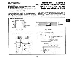
els in one pack- age, each channel consisting of a driver circuit controlling a SPST junction FET switch. The driver interfaces DTL, TTL, of RTL togic signals for multiplexing, commutating, and D/A converter applications, which permits logic design IH5005 IH5007 2-Channel Drivers with SPST FET Switches Gate Available AND directly with the switch function. Logic 1 at the input turns the FET switch ON, and Logic 0 turns it OFF. The gate lead of the FETs has been brought out to enable the application of a referral resistor for nulling offset voltage due to charge injection. Driver points are brought out to provide for the addition of external FETs for expansion capability. . PIN CONFIGURATIONS oriver [] uf] si []2 1a[] ns D1 QU 12 1 vo NIC 0 4 " i vt 83 q il VAEF (ENABLE) D3 Cl | iNy ORIVER [ ij G3 _ a = = ~~ ae oo OUTLINE DWG DD, PD, JD Vrer(ENABLE) INA G3 OUTLINE DWG FD-2 SCHEMATIC AND LOGIC DIAGRAMS 1H5005 (rpsion) = 10Q) 1H5006 (rpsjon) = 302) 1H5007 (rpsion) = 802) ve rn ' yo a 4 yh. : tLo4 : V
 4 Pages, 123 KB, Scan


