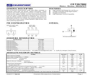
rol, power MOSFET gate drivers, and other switching applications. PIN CONFIGURATION SYMBOL SOT-23, SOT-323 SOT-363 Top View Top View D2 G1 D S1 1 G SOURCE DRAIN GATE 3 S2 2 G2 S D1 N-Channel MOSFET ORDERING INFORMATION Part Number Package CMT2N7002 SOT-23 CMT2N7002G* SOT-23 CMT2N7002WG* SOT-323 CMT2N7002DWG* SOT-363 CMT2N7002X* SOT-23 CMT2N7002WX* SOT-323 CMT2N7002DWX* SOT-363 *Note: G : Suffix for Pb Free Product W: Suffix for Package SOT-323 X : Suffix for Halogen Free Product ABSOLUTE MAXIMUM RATINGS Rating Symbol Value Unit Drain Source Voltage VDSS 60 V Drain-Gate Voltage (RGS = 1.0M) VDGR 60 V mA Drain to Current Continuous ID 115 IDM 800 VGS 20 VGSM 40 V PD 225 mW 1.8 mW/ EAS 9.6 mJ Operating and Storage Temperature Range TJ, TSTG -55 to 150 Thermal Resistance Junction to Ambient JA 417 /W Maximum Lead Temperature for Soldering Purposes, 1/8" from case for 10 seconds TL 300 Pulsed Gate-to-Source Voltage Continue Non-repetitive Total Power Dissipation Derate above 25 Single Pulse Drain-to-S
 6 Pages, 205 KB, Original
rol, power MOSFET gate drivers, and other switching applications. PIN CONFIGURATION SYMBOL SOT-23, SOT-323 SOT-363 Top View Top View D2 G1 D S1 1 G SOURCE DRAIN GATE 3 S2 2 G2 S D1 N-Channel MOSFET ORDERING INFORMATION Part Number Package CMT2N7002 SOT-23 CMT2N7002G* SOT-23 CMT2N7002WG* SOT-323 CMT2N7002DWG* SOT-363 CMT2N7002X* SOT-23 CMT2N7002WX* SOT-323 CMT2N7002DWX* SOT-363 *Note: G : Suffix for Pb Free Product W: Suffix for Package SOT-323 X : Suffix for Halogen Free Product ABSOLUTE MAXIMUM RATINGS Rating Symbol Value Unit Drain Source Voltage VDSS 60 V Drain-Gate Voltage (RGS = 1.0M) VDGR 60 V mA Drain to Current Continuous ID 115 IDM 800 VGS 20 VGSM 40 V PD 225 mW 1.8 mW/ EAS 9.6 mJ Operating and Storage Temperature Range TJ, TSTG -55 to 150 Thermal Resistance Junction to Ambient JA 417 /W Maximum Lead Temperature for Soldering Purposes, 1/8" from case for 10 seconds TL 300 Pulsed Gate-to-Source Voltage Continue Non-repetitive Total Power Dissipation Derate above 25 Single Pulse Drain-to-S
 6 Pages, 209 KB, Original
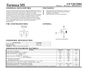
 applications such as small servo motor control, power MOSFET gate drivers, and other switching applications. PIN CONFIGURATION SYMBOL SOT-23 D Top View 1 G SOURCE DRAIN GATE 3 S 2 N-Channel MOSFET ORDERING INFORMATION Part Number Package CMT2N7002 SOT-23 CMT2N7002G* *Note: G : Suffix for Pb Free Product SOT-23 ABSOLUTE MAXIMUM RATINGS Rating Symbol Value Unit Drain Source Voltage VDSS 60 V Drain-Gate Voltage (RGS = 1.0M) VDGR 60 V ID 115 mA Drain to Current Continuous Pulsed IDM 800 VGS 20 VGSM 40 V PD 225 mW 1.8 mW/ EAS 9.6 mJ Operating and Storage Temperature Range TJ, TSTG -55 to 150 Thermal Resistance Junction to Ambient JA 417 /W Maximum Lead Temperature for Soldering Purposes, 1/8" from case for 10 seconds TL 300 Gate-to-Source Voltage Continue Non-repetitive Total Power Dissipation Derate above 25 Single Pulse Drain-to-Source Avalanche Energy TJ = 25 V (VDD = 50V, VGS = 10V, IAS = 0.8A, L = 30mH, RG = 25) CMT2N7002 Formosa MS SMALL SIGNAL MOSFET ELECTRICAL CHARACTERISTICS Unless otherwise
 4 Pages, 140 KB, Original


