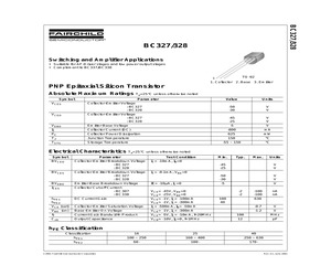
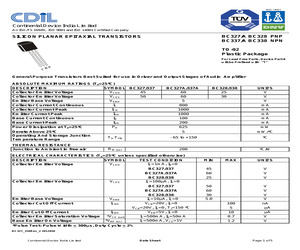
Driver stages and low power output stages * Complement to BC337/BC338 TO-92 1 1. Collector 2. Base 3. Emitter PNP Epitaxial Silicon Transistor Absolute Maximum Ratings Ta=25C unless otherwise noted Symbol VCES Parameter Collector-Emitter Voltage : BC327 : BC328 Value Units -50 -30 V V -45 -25 V V Collector-Emitter Voltage : BC327 : BC328 VCEO VEBO Emitter-Base Voltage -5 V IC Collector Current (DC) -800 mA PC Collector Power Dissipation 625 mW TJ Junction Temperature 150 C TSTG Storage Temperature -55 ~ 150 C Electrical Characteristics Ta=25C unless otherwise noted Symbol BVCEO Parameter Collector-Emitter Breakdown Voltage : BC327 : BC328 Test Condition IC= -10mA, IB=0 Collector-Emitter Breakdown Voltage : BC327 : BC328 IC= -0.1mA, VBE=0 BVEBO Emitter-Base Breakdown Voltage IE= -10A, IC=0 ICES Collector Cut-off Current : BC307 : BC338 VCE= -45V, VBE=0 VCE= -25V, VBE=0 BVCES hFE1 hFE2 Min. Typ. VCE= -1V, IC= -100mA VCE= -1V, IC= -300mA Units -45 -25 V V -50 -
 9 Pages, 139 KB, Original
Driver stages and low power output stages * Complement to BC337/BC338 TO-92 1 1. Collector 2. Base 3. Emitter PNP Epitaxial Silicon Transistor Absolute Maximum Ratings Ta=25C unless otherwise noted Symbol VCES Parameter Collector-Emitter Voltage : BC327 : BC328 Value Units -50 -30 V V -45 -25 V V Collector-Emitter Voltage : BC327 : BC328 VCEO VEBO Emitter-Base Voltage -5 V IC Collector Current (DC) -800 mA PC Collector Power Dissipation 625 mW TJ Junction Temperature 150 C TSTG Storage Temperature -55 ~ 150 C Electrical Characteristics Ta=25C unless otherwise noted Symbol BVCEO Parameter Collector-Emitter Breakdown Voltage : BC327 : BC328 Test Condition IC= -10mA, IB=0 Collector-Emitter Breakdown Voltage : BC327 : BC328 IC= -0.1mA, VBE=0 BVEBO Emitter-Base Breakdown Voltage IE= -10A, IC=0 ICES Collector Cut-off Current : BC327 : BC328 VCE= -45V, VBE=0 VCE= -25V, VBE=0 BVCES hFE1 hFE2 Min. Typ. VCE= -1V, IC= -100mA VCE= -1V, IC= -300mA Units -45
 7 Pages, 186 KB, Original
23 SOT23R SOT23 SOT23R SOT23 SOT23 SOT323 SOT23 SOT89 SOT23R SOT23 SOT23 SOT323 SOT23R SOT23 SOT23 SOT23 SOT23 SOT23 SOT23 SOT23 SOT23R SOT23R SOT23R SOT346 SOT346 SOT23R SOT89 SOT89 BC327-40 1N914 1N914 1N914 dual cc HD2 75V 100mA BC327 BC327 BC327 BC327 BC328-16 BC328-16 BC328-16 MPSA43 BC328-16 BC328-16 BC328-25 BC328-25 BC328-25 MBD501 hot carrier diode DC-4GHz MMIC amp 20 dB gain BC328-25 BC328-40 BC328-40 BC328-40 dual series MBD101 BC328-40 MBD701 UHF schottky diode BC328 BC328 1N4148 1N4148 BCX38B Hyperabrupt varicap dual cc 3GHz RF pin diode dual cc Hyperabrupt varicap series UHF schottky diodes 2N2907A npn 45V 0.8A 350mW npn 32V 0.8A 5.1V 0.3W zener 5.6V 0.3W zener pnp 32V 0.8A 5.1V 1W zener 5.6V 1W zener Codes beginning with '6' Code 6 (red) 60s 605 61s 61A 61C 61A 61J 61K 61L 61M 61N 61P 61Q 61S 61T Device
 80 Pages, 1313 KB, Original
N N C AZ R N N N D R C N N C C N C B B D R R R C C R O O SOT23 SOT23 SOT323 SOT23R SOT23 SOT23R SOT23 SOT23 SOT323 SOT23 SOT89 SOT23R SOT23 SOT23 SOT323 SOT23R SOT23 SOT23 SOT23 SOT23 SOT23 SOT23 SOT23 SOT23R SOT23R SOT23R SOT346 SOT346 SOT23R SOT89 SOT89 BC328-16 BC328-16 BC328-16 MPSA43 BC328-16 BC328-16 BC328-25 BC328-25 BC328-25 MBD501 hot carrier diode DC-4GHz MMIC amp 20 dB gain BC328-25 BC328-40 BC328-40 BC328-40 dual series MBD101 BC328-40 MBD701 UHF schottky diode BC328 BC328 1N4148 1N4148 BCX38B Hyperabrupt varicap dual cc 3GHz RF pin diode dual cc Hyperabrupt varicap series UHF schottky diodes 2N2907A npn 45V 0.8A 350mW npn 32V 0.8A 5.1V 0.3W zener 5.6V 0.3W zener pnp 32V 0.8A 5.1V 1W zener 5.6V 1W zener Codes beginning with '6' Code 6 (red) 60s 605 61s 61A 61C 61A 61J 61K 61L 61M 61N 61P 61Q 61S 61T 61U 61
 80 Pages, 1517 KB, Original
T23E BC327-40 5D FMMD914 Zet C SOT23 1N914 5D MMBD914 Mot C SOT23 1N914 5D MMSD914 Mot I SOD123 1N914 5D HD2A Zet B 5Dp BC807 Phi N SOT23 BC327 5Dt BC807 Phi N SOT23 BC327 5Dt BC807W Phi N SOT323 BC327 5D- BC807W Phi N SOT323 BC327 5E BC808-16 Phi N SOT23 BC328-16 5E CDZ6.8B Roh I VMN2 zener 6.8V 0.15W 5Es BC808-16 Sie N SOT23 BC328-16 5Es BC808-16W Sie N SOT323 BC328-16 5E FMMT-A43R Zet R SOT23R MPSA43 5E BC808-16 Phi N SOT23 BC328-16 5ER BC808-16R Phi R SOT23R BC328-16 5F BC808-25 Phi N SOT23 BC328-25 5F CDZ7.5B Roh I VMN2 zener 7.5V 0.15W dual cc HD2 75V 100mA http://www.marsport.org.uk/smd/smd5.htm (4 of 5)27/5/2007 18:19:02 SMD Codebook Page 5 5Fs BC808-25 Sie N SOT23 BC328-25 5Fs BC808-25W Sie N SOT323 BC328-25 5F MMBD501 Mot C SOT23 MBD501 hot carrier diode 5F Gali-5F MC AZ SOT89 DC-4GHz MMIC amp 20 dB gain 5FR BC808-25R Phi R SOT23R BC328-25 5G BC808-40 Phi N SOT23 BC328-40
 229 Pages, 2019 KB, Original
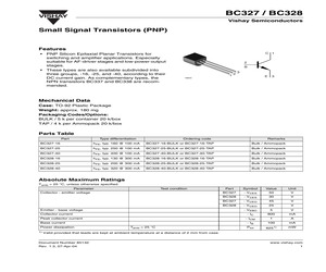
BC328 VISHAY Vishay Semiconductors Small Signal Transistors (PNP) Features * PNP Silicon Epitaxial Planar Transistors for switching and amplifier applications. Especially suitable for AF-driver stages and low-power output stages. * These types are also available subdivided into three groups, -16, -25, and -40, according to their DC current gain. As complementary types, the NPN transistors BC337 and BC338 are recommended. C 1 2 B 18855 1 2 3 E 3 Mechanical Data Case: TO-92 Plastic Package Weight: approx. 180 mg Packaging Codes/Options: BULK / 5 k per container 20 k/box TAP / 4 k per Ammopack 20 k/box Parts Table Part Type differentiation Ordering code Remarks BC327-16 hFE, typ. 160 @ 100 mA BC327-16-BULK or BC327-16-TAP Bulk / Ammopack BC327-25 hFE, typ. 250 @ 100 mA BC327-25-BULK or BC327-25-TAP Bulk / Ammopack BC327-40 hFE, typ. 400 @ 100 mA BC327-40-BULK or BC327-40-TAP Bulk / Ammopack BC328-16 hFE, typ. 130 @ 300 mA BC328-16-BULK or BC328-16-TAP Bulk / Am
 7 Pages, 131 KB, Original
BC328 VISHAY Vishay Semiconductors Small Signal Transistors (PNP) Features * PNP Silicon Epitaxial Planar Transistors for switching and amplifier applications. Especially suitable for AF-driver stages and low-power output stages. * These types are also available subdivided into three groups, -16, -25, and -40, according to their DC current gain. As complementary types, the NPN transistors BC337 and BC338 are recommended. C 1 2 B 18979 1 2 3 E 3 Mechanical Data Case: TO-92 Plastic Package Weight: approx. 177 mg Packaging Codes/Options: BULK / 5 k per container 20 k/box TAP / 4 k per Ammopack 20 k/box Parts Table Part Type differentiation Ordering code Remarks BC327-16 hFE, typ. 160 @ 100 mA BC327-16-BULK or BC327-16-TAP Bulk / Ammopack BC327-25 hFE, typ. 250 @ 100 mA BC327-25-BULK or BC327-25-TAP Bulk / Ammopack BC327-40 hFE, typ. 400 @ 100 mA BC327-40-BULK or BC327-40-TAP Bulk / Ammopack BC328-16 hFE, typ. 130 @ 300 mA BC328-16-BULK or BC328-16-TAP Bulk / Am
 7 Pages, 130 KB, Original
ual diode 70V 0.2A cc dual diode 70V 0.2A cc dual diode 70V 0.2A BC327-25 BC327-40 BC327-40 BC327-40 BC327-40 BC327-40 BC327-40 BC327-40 2 ser diodes 100V 0.2A 2 ser diodes 70V 200mA BC327-40 1N914 1N914 1N914 dual cc HD2 75V 100mA BC327 BC327 BC327 BC327 BC328-16 BC328-16 BC328-16 MPSA43 BC328-16 BC328-16 BC328-25 BC328-25 BC328-25 MBD501 hot carrier diode DC-4GHz MMIC amp 20 dB gain BC328-25 BC328-40 BC328-40 BC328-40 dual series MBD101 BC328-40 MBD701 UHF schottky diode BC328 BC328 1N4148 1N4148 BCX38B Hyperabrupt varicap dual cc 3GHz RF pin diode dual cc Hyperabrupt varicap series UHF schottky diodes 2N2907A npn 45V 0.8A 350mW npn 32V 0.8A 5.1V 0.3W zener 5V6 5W 5Y1 5Y6 PZM5.6NB BCW67BR BZV49-C5V1 BZV49-C5V6 Phi Zet Phi Phi C R O O SOT346 SOT23R SOT89 SOT89 5.6V 0.3W zener pnp 32V 0.8A 5.1V 1W zener 5.6V 1W zener
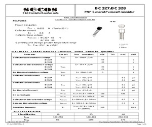
 95 Pages, 1386 KB, Original
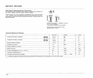
BC328 PNP general purpose transistors Product specification Supersedes data of September 1994 File under Discrete Semiconductors, SC04 1997 Mar 10 Philips Semiconductors Product specification BC327; BC327A; BC328 PNP general purpose transistors FEATURES PINNING * High current (max. 500 mA) PIN * Low voltage (max. 60 V). APPLICATIONS DESCRIPTION 1 emitter 2 base 3 collector * General purpose switching and amplification, e.g. driver and output stages of audio amplifiers. DESCRIPTION handbook, halfpage1 PNP transistor in a TO-92; SOT54 plastic package. NPN complements: BC337, BC337A and BC338. 3 2 3 2 1 MAM281 Fig.1 Simplified outline (TO-92; SOT54) and symbol. QUICK REFERENCE DATA SYMBOL VCBO PARAMETER collector-base voltage CONDITIONS - -50 V BC327A - -60 V - -30 V - -45 V collector-emitter voltage open base BC327A - -60 V BC328 - -25 V - -1 A - 625 mW 100 600 100 400 80 - ICM peak collector current Ptot total power dissipation Tamb 25 C hFE DC current gain IC = -100 mA;
 8 Pages, 56 KB, Original
2 30-06-99 31-12-99 BC327 M, 6 Type insufficient Volume, Standard EOL 2953 BC327A SOT54 Transistor 933643190116 30-06-99 31-12-99 BC327 M, 6 Type insufficient Volume, Standard EOL 2954 BC327A SOT54 Transistor 933643190126 30-06-99 31-12-99 BC327 M, 6 2955 BC328 SOT54 Transistor 933149190112 30-06-99 31-12-99 BC327 M, 6 2956 BC328 SOT54 Transistor 933149190116 30-06-99 31-12-99 BC327 M, 6 2957 BC328 SOT54 Transistor 933149190126 30-06-99 31-12-99 BC327 M, 6 2958 BC328-16 SOT54 Transistor 933179550112 30-06-99 31-12-99 BC327-16 M, 6 2959 BC328-16 SOT54 Transistor 933179550116 30-06-99 31-12-99 BC327-16 M, 6 2960 BC328-16 SOT54 Transistor 933179550126 30-06-99 31-12-99 BC327-16 M, 6 2961 BC328-25 SOT54 Transistor 933179560112 30-06-99 31-12-99 BC327-25 M, 6 2962 BC328-25 SOT54 Transistor 933179560116 30-06-99 31-12-99 BC327-25 M, 6 2963 BC328-25 SOT54 Transistor 933179560126 30-06-99 31-12-99 BC32
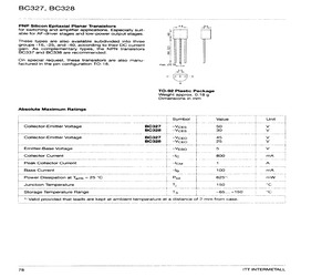
 179 Pages, 400 KB, Original
BC328 PNP Silicon Epitaxial Planar Transistors for switching and amplifier applications. Especially suitable for AF-driver stages and low power output stages. These types are also available subdivided into three groups 16, 25 and 40, according to their DC current gain. As com- plementary types the NPN transistors BC337 and BC338 are recommended. Absolute Maximum Ratings B E-(ele)-c oF 25 4 oo min.12,5-1 46 max25e! le [ max.05 425 Plastic Package ~ JEDEC TO-92 TO-18 compatible The case is impervious to light Weight approximately 0.18 g Dimensions in mm Symbol Value Unit Collector Emitter Voltage BC327 Voces 50 V BC328 ~Voes 30 V Collector Emitter Voltage BC327 Vceo 45 Vv BC328 Vceo 25 Vv Emitter Base Voltage VeBo 5 Vv Collector Current -Ic 800 mA Peak Collector Current lom 1 A Base Current lp 100 mA Power Dissipation at Tamp = 25 C Prot 625") mW Junction Temperature T; 150 C Storage Temperature Range Ts 55...+150 C ) Valid provided that leads are kept at ambient temperatu
 5 Pages, 149 KB, Scan
PS2222A 2N4401 2N4400 MPS6602 2N3903 2N3904 BC548 BC548A BC548B BC548C 2N4123 2N4124 BC338 MPS8599 MPSA56 -- BC556 BC556B MPSA55 MPS2907A BC212 BC307B BC327 BC557 BC557A BC557B BC557C MPSA70 -- 2N4403 2N4402 MPS6652 2N3905 2N3906 -- -- BC558B -- 2N4125 -- BC328 80 80 80 65 65 60 60 50 45 45 45 45 45 45 40 40 40 40 40 40 40 30 30 30 30 30 25 25 150 100 60 150 150 100 200 200(1) 150 210(1) 150 150 150 150 125 300 200 150 100 200 250 300(1) 300(1) 300(1) 300 200 250 210(1) (1) Typical Devices listed in bold, italic are Motorola preferred devices. Selector Guide 1-2 Motorola Small-Signal Transistors, FETs and Diodes Device Data Plastic-Encapsulated Transistors (continued) Table 1. Plastic-Encapsulated General-Purpose Transistors (continued) NPN PNP V(BR)CEO Volts Min fT @ IC MHz Min hFE @ IC VCE(sat) @ IC @ IB mA IC A Max Min Max mA Volts Max mA mA Style 200 200 200 200 0.5 0.5 0.5 0.5 40 40 80 80 400 400 -- -- 100 100 50 50 0.7 0.7 0.5 0.4 1000 1000 250 250 100 100 10 10 14 1 1 1 Case 29-05 -- TO-22
 1354 Pages, 24604 KB, Original
BC328 PNP BC337/A BC338 NPN SILICON PLANAR EPITAXIAL TRANSISTORS TO-92 Plastic Package For Lead Free Parts, Device Part # will be Prefixed with "T" C BE General Purpose Transistors Best Suited for use in Driver and Output Stages of Audio Amplifier ABSOLUTE MAXIMUM RATINGS (Ta=25C) DESCRIPTION Collector Emitter Voltage Collector Emitter Voltage Emitter Base Voltage Collector Current Continuous Collector Current Peak Emitter Current Peak Base Current Continuous Base Current Peak Power Dissipation at Ta=25C Derate Above 25C Operating And Storage Junction Temperature Range THERMAL RESISTANCE Junction to Ambient in free air SYMBOL BC327/337 VCEO 45 VCES 50 VEBO IC ICM IEM IB IBM PD BC327A/337A 60 60 5 800 1000 1000 100 200 625 BC328/338 25 30 UNITS V V V mA mA mA mA mA mW 5 mW/C Tj, Tstg - 65 to +150 C Rth (j-a) 200 C/W ELECTRICAL CHARACTERISTICS (Ta=25C unless specified otherwise) DESCRIPTION Collector Emitter Voltage MAX SYMBOL VCEO TEST CONDITION IC=1mA, IB=0 MIN 45 60 25 V V V VCES BC
 5 Pages, 348 KB, Original
BC328 PNP General PurposeTransistor Elektronische Bauelemente RoHS Compliant Product A suffix of "-C" specifies halogen & lead-free FEATURES TO-92 Power dissipation PCM : 0.625 WTamb=25 Collector current ICM : -0.8 A Collector-base voltage V(BR)CBO : BC327 -50 V 1 2 3 1 2 3 BC328 -30 Operating and storage junction temperature range 1. COLLECTOR T J T stg: -55 to +150 2. BASE 3 . EMITTER . ELECTRICAL CHARACTERISTICS (Tamb=25 unless otherwise specified) Parameter Symbol VCBO Collector-base breakdown voltage Test conditions MIN TYP MAX UNIT Ic= -100A , IE=0 BC327 -50 V BC328 -30 V -45 V -25 V -5 V IC= -10 mA , IB=0 Collector-emitter breakdown voltage VCEO BC327 BC328 Emitter-base breakdown voltage VEBO Collector cut-off current ICBO IE= -10A, IC=0 BC327 VCB= -45V, IE=0 -0.1 A BC328 VCB= -25V, IE=0 -0.1 A VCE= -40V, IB=0 -0.2 A VCE= -20 V, IB=0 -0.2 A IEBO VEB= -4 V, IC=0 -0.1 A hFE(1) VCE=-1V, IC= -100mA 100 hFE(2) VCE=-1V, IC= -300mA 40 Collector-
 3 Pages, 103 KB, Original
BC328 PNP Silicon Epitaxial Planar Transistors for switching and amplifier applications. Especially suit- able for AF-driver stages and low-power output stages. These types are aiso available subdivided into three groups -16, -25, and -40, according to their DC current gain. As complementary types, the NPN transistors BC337 and BC338 are recommended. On special request, these transistors are also manu- factured in the pin configuration TO-18. Absolute Maximum Ratings al 46 in 12.5 =_ TO-92 Plastic Package Weight approx. 0.18 g Dimensions in mm Unit | | Collector-Emitter Voltage _ Be327 -Vces a 50 : Vv _ 7 BC328 = -Vces_ ss 30 Vv Collector-Emitter Voltage _ BC327 -VoEo : - 45 ; - yo / BC328 ~VcEO 25 V Emitter-Base Voltage i -VEBO 5 : oy ; : Collector Current | i a 800 a mA. | | Peak Collector Current - - - lon ; 1 Oo - A : Base Current : lp op 400. a : mA - Power Dissipation at Tamb = 25 C a : Prot | i 6250) - mW. Junction Temperature 7 T; 150 8S Storage Temperature Range
 5 Pages, 185 KB, Scan


