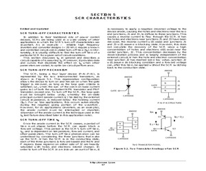
cal inductor L1 is used, a clamp diode, scaled to the diverted current, should be placed across L1 to limit "inductive kicks." shown in Figure 5.7 where both a fast recovery rectifier and standard recovery rectifier were used in measuring tq of a standard 2N6508 SCR. Although the di/dt's were the same, the reverse recovery current IRM and trr were greater with the standard recovery rectifier, resulting in a somewhat shorter tq (59 s versus 63 s). In fact, tq is affected by the initial conditions (ITM, di/dt, IRM, dv/dt, etc.) and these conditions should be specified to maintain measurement repeatability. This is later described in the published curves and tables. Finally, the resistor R1 and the resultant current I1 in the dv/dt circuit must meet certain criteria: I1 should be greater than the SCR holding current so that when the DUT does indicate tq limitation, it latches up, thus suppressing the dv/dt ramp voltage; and, for fast SCRs (low tq), I1 should be large enough to ensure measurement rep
 674 Pages, 7097 KB, Original
cal inductor L1 is used, a clamp diode, scaled to the diverted current, should be placed across L1 to limit "inductive kicks." shown in Figure 5.7 where both a fast recovery rectifier and standard recovery rectifier were used in measuring tq of a standard 2N6508 SCR. Although the di/dt's were the same, the reverse recovery current IRM and trr were greater with the standard recovery rectifier, resulting in a somewhat shorter tq (59 s versus 63 s). In fact, tq is affected by the initial conditions (ITM, di/dt, IRM, dv/dt, etc.) and these conditions should be specified to maintain measurement repeatability. This is later described in the published curves and tables. Finally, the resistor R1 and the resultant current I1 in the dv/dt circuit must meet certain criteria: I1 should be greater than the SCR holding current so that when the DUT does indicate tq limitation, it latches up, thus suppressing the dv/dt ramp voltage; and, for fast SCRs (low tq), I1 should be large enough to ensure measurement rep
 674 Pages, 7093 KB, Original
cal inductor L1 is used, a clamp diode, scaled to the diverted current, should be placed across L1 to limit "inductive kicks." shown in Figure 5.7 where both a fast recovery rectifier and standard recovery rectifier were used in measuring tq of a standard 2N6508 SCR. Although the di/dt's were the same, the reverse recovery current IRM and trr were greater with the standard recovery rectifier, resulting in a somewhat shorter tq (59 s versus 63 s). In fact, tq is affected by the initial conditions (ITM, di/dt, IRM, dv/dt, etc.) and these conditions should be specified to maintain measurement repeatability. This is later described in the published curves and tables. Finally, the resistor R1 and the resultant current I1 in the dv/dt circuit must meet certain criteria: I1 should be greater than the SCR holding current so that when the DUT does indicate tq limitation, it latches up, thus suppressing the dv/dt ramp voltage; and, for fast SCRs (low tq), I1 should be large enough to ensure measurement rep
 240 Pages, 2542 KB, Original
cal inductor L1 is used, a clamp diode, scaled to the diverted current, should be placed across L1 to limit "inductive kicks." shown in Figure 5.7 where both a fast recovery rectifier and standard recovery rectifier were used in measuring tq of a standard 2N6508 SCR. Although the di/dt's were the same, the reverse recovery current IRM and trr were greater with the standard recovery rectifier, resulting in a somewhat shorter tq (59 s versus 63 s). In fact, tq is affected by the initial conditions (ITM, di/dt, IRM, dv/dt, etc.) and these conditions should be specified to maintain measurement repeatability. This is later described in the published curves and tables. Finally, the resistor R1 and the resultant current I1 in the dv/dt circuit must meet certain criteria: I1 should be greater than the SCR holding current so that when the DUT does indicate tq limitation, it latches up, thus suppressing the dv/dt ramp voltage; and, for fast SCRs (low tq), I1 should be large enough to ensure measurement rep
 33 Pages, 299 KB, Original
cal inductor L1 is used, a clamp diode, scaled to the diverted current, should be placed across L1 to limit "inductive kicks." shown in Figure 5.7 where both a fast recovery rectifier and standard recovery rectifier were used in measuring tq of a standard 2N6508 SCR. Although the di/dt's were the same, the reverse recovery current IRM and trr were greater with the standard recovery rectifier, resulting in a somewhat shorter tq (59 s versus 63 s). In fact, tq is affected by the initial conditions (ITM, di/dt, IRM, dv/dt, etc.) and these conditions should be specified to maintain measurement repeatability. This is later described in the published curves and tables. Finally, the resistor R1 and the resultant current I1 in the dv/dt circuit must meet certain criteria: I1 should be greater than the SCR holding current so that when the DUT does indicate tq limitation, it latches up, thus suppressing the dv/dt ramp voltage; and, for fast SCRs (low tq), I1 should be large enough to ensure measurement rep
 241 Pages, 2879 KB, Original
006 - Rev. 8 1 Publication Order Number: 2N6504/D 2N6504 Series MAXIMUM RATINGS (TJ = 25C unless otherwise noted) Symbol Rating Value Unit *Peak Repetitive Off-State Voltage (Note 1) (Gate Open, Sine Wave 50 to 60 Hz, TJ = 25 to 125C) 2N6504 2N6505 2N6507 2N6508 2N6509 VDRM, VRRM V OnState Current RMS (180 Conduction Angles; TC = 85C) IT(RMS) 25 A Average OnState Current (180 Conduction Angles; TC = 85C) IT(AV) 16 A Peak Nonrepetitive Surge Current (1/2 Cycle, Sine Wave 60 Hz, TJ = 100C) ITSM 250 A Forward Peak Gate Power (Pulse Width 1.0 ms, TC = 85C) PGM 20 W PG(AV) 0.5 W 50 100 400 600 800 Forward Average Gate Power (t = 8.3 ms, TC = 85C) Forward Peak Gate Current (Pulse Width 1.0 ms, TC = 85C) IGM 2.0 A Operating Junction Temperature Range TJ -40 to +125 C Storage Temperature Range Tstg -40 to +150 C Stresses exceeding Maximum Ratings may damage the device. Maximum Ratings are stress ratings only. Functional operation above the Recommended Operating Conditions is not implied. Extended exposur
 8 Pages, 86 KB, Original
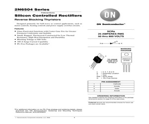
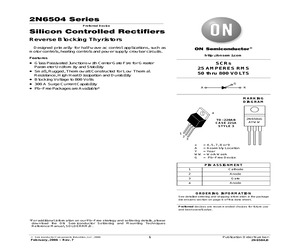
Date Code http://onsemi.com SCRs 25 AMPERES RMS 50 thru 800 VOLTS G A MAXIMUM RATINGS (TJ = 25C unless otherwise noted) Rating Symbol Value Unit *Peak Repetitive Off-State Voltage(1) (Gate Open, Sine Wave 50 to 60 Hz, TJ = 25 to 125C) 2N6504 2N6505 2N6507 2N6508 2N6509 VDRM, VRRM On-State RMS Current (180 Conduction Angles; TC = 85C) IT(RMS) 25 Average On-State Current (180 Conduction Angles; TC = 85C) IT(AV) 16 Peak Non-repetitive Surge Current 8.3 ms (1/2 Cycle, Sine Wave 60 Hz, TJ = 85C) 1.5 ms ITSM Forward Peak Gate Power (Pulse Width 1.0 s, TC = 85C) PGM 20 Watts PG(AV) 0.5 Watts IGM 2.0 A TJ - 40 to +125 C - 40 to +150 C Forward Average Gate Power (t = 8.3 ms, TC = 85C) Forward Peak Gate Current (Pulse Width 1.0 s, TC = 85C) Operating Junction Temperature Range Storage Temperature Range K Volts 4 50 100 400 600 800 A 1 A 2 3 TO-220AB CASE 221A STYLE 3 A 300 PIN ASSIGNMENT 350 Tstg 1 Cathode 2 Anode 3 Gate 4 Anode ORDERING INFORMATION Device *Indicates JEDEC Registered Data (1) VDRM and VRRM
 14 Pages, 85 KB, Original
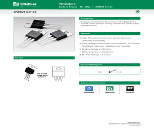
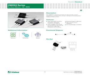
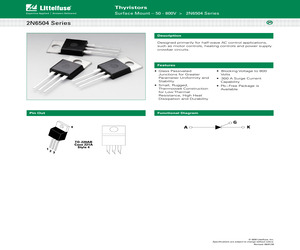
ifications are subject to change without notice. Revised: 02/28/19 Thyristors Surface Mount - 50 - 800V > 2N6504 Series Maximum Ratings (TJ = 25C unless otherwise noted) Rating Symbol Value Unit VDRM, VRRM 50 100 400 600 800 V IT 25 A 2N6504 2N6505 2N6507 2N6508 2N6509 Peak Repetitive Off-State Voltage (Note 1) (Gate Open, Sine Wave 50 to 60 Hz, TJ = 25 to 125C) On-State RMS Current (180 Conduction Angles; TC = 85C) (RMS) Average On-State Current (180 Conduction Angles; TC = 85C) IT (AV) 16 A Peak Non-repetitive Surge Current (1/2 Cycle, Sine Wave 60 Hz, TJ = 100C) ITSM 250 As Forward Peak Gate Power (Pulse Width 1.0 s, TC = 85C) PGM 20 W Forward Average Gate Power (t = 8.3 ms, TC = 85C) PG(AV) 0.5 W Forward Peak Gate Current (Pulse Width 1.0 s, TC = 85C) IGM 2.0 A Operating Junction Temperature Range TJ -40 to +125 C Storage Temperature Range Tstg -40 to +125 C Stresses exceeding Maximum Ratings may damage the device. Maximum Ratings are stress ratings only. Functional operation above the Recomm
 6 Pages, 637 KB, Original
006 - Rev. 8 1 Publication Order Number: 2N6504/D 2N6504 Series MAXIMUM RATINGS (TJ = 25C unless otherwise noted) Symbol Rating Value Unit *Peak Repetitive Off-State Voltage (Note 1) (Gate Open, Sine Wave 50 to 60 Hz, TJ = 25 to 125C) 2N6504 2N6505 2N6507 2N6508 2N6509 VDRM, VRRM V OnState Current RMS (180 Conduction Angles; TC = 85C) IT(RMS) 25 A Average OnState Current (180 Conduction Angles; TC = 85C) IT(AV) 16 A Peak Nonrepetitive Surge Current (1/2 Cycle, Sine Wave 60 Hz, TJ = 100C) ITSM 250 A Forward Peak Gate Power (Pulse Width 1.0 ms, TC = 85C) PGM 20 W PG(AV) 0.5 W 50 100 400 600 800 Forward Average Gate Power (t = 8.3 ms, TC = 85C) Forward Peak Gate Current (Pulse Width 1.0 ms, TC = 85C) IGM 2.0 A Operating Junction Temperature Range TJ -40 to +125 C Storage Temperature Range Tstg -40 to +150 C Stresses exceeding Maximum Ratings may damage the device. Maximum Ratings are stress ratings only. Functional operation above the Recommended Operating Conditions is not implied. Extended exposur
 7 Pages, 81 KB, Original
EVICE Deletions (Cont) DEVICE Deletions (Cont) DEVICE 2N4401RLRPG 2N4403G 2N4403RLRAG 2N4403RLRPG 2N5061RLRAG 2N5062RLRAG 2N5064RLRMG 2N5089G 2N5089RLRAG 2N5089RLREG 2N5401G 2N5551G 2N5551RLRPG 2N6028G 2N6073BG 2N6075AG 2N6394G 2N6426G 2N6427RLRAG 2N6504G 2N6508G 2SA1162GT1 2SA1162YT1 2SA1774G 2SA2029M3T5G 2SC4617G 2SC5658M3T5G 74VCXH245MNR2G CS5204-2GDP3 CS5204-3GDPR3 CS5204-3GDP3 CS5205-1GDPR3 CS5205-1GDP3 CS5205-2GDPR3 CS5205-2GDP3 CS5205-3GDPR3 CS5205-3GDP3 CS5205A-1GDPR3 CS5205A-1GDP3 CS5206-3GDPR3 CS5206-3GDP3 CS5207-3GDPR3 CS5207-3GDP3 CS5211EDR14 CS5211ED14 CS5211GDR14 CS5211GD14 CS5212EDR14 CS5212ED14 CS5212GDR14 CS5212GD14 CS5231-3GDPR5 CS5231-3GDP5 CS5233-3GDPR5 CS5233-3GDP5 CS5253B-1GDPR5 CS5253B-1GDP5 CS5253B-8GDPR5 CS5253B-8GDPR5G CS5253B-8GDP5 CS5253B-8GDP5G CS5257A-1GDPR5 CS5257A-1GDP5 CS8126-1YDPSR7G LM2575TV-ADJG LM2575TV-005G LM2576TV-ADJ LM2576TV-ADJG LM2576TV-005 LM2576TV-3.3 MBRB20H100CT MBRB20H100CTT4 MBRS2H40LT3 MBR1545CTP MBR2045CTP MBR2545CTP MC33567D-002 MC33567D-2R2 MC
 296 Pages, 947 KB, Original
urface Mount - 50 - 800V > 2N6504 Series Maximum Ratings (TJ = 25C unless otherwise noted) Rating Symbol Value Unit 2N6504 VDRM, 2N6505 VRRM 50 100 V Peak Repetitive Off-State Voltage (Note 1) (Gate Open, Sine Wave 50 to 60 Hz, TJ = 25 to 125C) 2N6507 400 2N6508 600 2N6509 800 On-State RMS Current (180 Conduction Angles; TC = 85C) IT (RMS) 25 A Average On-State Current (180 Conduction Angles; TC = 85C) IT (AV) 16 A Peak Non-repetitive Surge Current (1/2 Cycle, Sine Wave 60 Hz, TJ = 100C) ITSM 250 As Forward Peak Gate Power (Pulse Width 1.0 s, TC = 85C) PGM 20 W Forward Average Gate Power (t = 8.3 ms, TC = 85C) PG(AV) 0.5 W Forward Peak Gate Current (Pulse Width 1.0 s, TC = 85C) IGM 2.0 A Operating Junction Temperature Range TJ -40 to +125 C Storage Temperature Range Tstg -40 to +125 C Stresses exceeding Maximum Ratings may damage the device. Maximum Ratings are stress ratings only. Functional operation above the Recommended Operating Conditions is not implied. Extended exposure to stresses above
 7 Pages, 913 KB, Original
 Semiconductor Components Industries, LLC, 2008 1 2N6504 Series MAXIMUM RATINGS (TJ = 25C unless otherwise noted) Rating Symbol Value Unit *Peak Repetitive Off-State Voltage (Note 1) (Gate Open, Sine Wave 50 to 60 Hz, TJ = 25 to 125C) 2N6504 2N6505 2N6507 2N6508 2N6509 VDRM, VRRM V OnState Current RMS (180 Conduction Angles; TC = 85C) IT(RMS) 25 A Average OnState Current (180 Conduction Angles; TC = 85C) IT(AV) 16 A Peak Nonrepetitive Surge Current (1/2 Cycle, Sine Wave 60 Hz, TJ = 100C) ITSM 250 A Forward Peak Gate Power (Pulse Width 1.0 ms, TC = 85C) PGM 20 W PG(AV) 0.5 W 50 100 400 600 800 Forward Average Gate Power (t = 8.3 ms, TC = 85C) Forward Peak Gate Current (Pulse Width 1.0 ms, TC = 85C) IGM 2.0 A Operating Junction Temperature Range TJ -40 to +125 C Storage Temperature Range Tstg -40 to +150 C Stresses exceeding Maximum Ratings may damage the device. Maximum Ratings are stress ratings only. Functional operation above the Recommended Operating Conditions is not implied. Extended exposur
 5 Pages, 71 KB, Original
221A Style 4 23 (c) 2021 Littelfuse, Inc. Specifications are subject to change without notice. Revised: GD. 02/12/21 Thyristors Datasheet 2N6504 Series Surface Mount - 50 - 800V Maximum Ratings (TJ = 25C unless otherwise noted) Rating 2N6504 2N6505 2N6507 2N6508 2N6509 Peak Repetitive Off-State Voltage (Note 1) (Gate Open, Sine Wave 50 to 60 Hz, TJ = 25 to 125C) On-State RMS Current (180 Conduction Angles; TC = 85C) Symbol Value Unit VDRM, VRRM 50 100 400 600 800 V IT 25 A Average On-State Current (180 Conduction Angles; TC = 85C) IT (AV) 16 A Peak Non-repetitive Surge Current (1/2 Cycle, Sine Wave 60 Hz, TJ = 100C) ITSM 250 A (RMS) Forward Peak Gate Power (Pulse Width 1.0 s, TC = 85C) PGM 20 W Forward Average Gate Power (t = 8.3 ms, TC = 85C) PG(AV) 0.5 W Forward Peak Gate Current (Pulse Width 1.0 s, TC = 85C) IGM 2.0 A Operating Junction Temperature Range TJ -40 to +125 C Storage Temperature Range Tstg -40 to +150 C Stresses exceeding Maximum Ratings may damage the device. Maximum Ratings are s
 6 Pages, 476 KB, Original
 Specifications are subject to change without notice. Revised: 09/01/20 Thyristors Surface Mount - 50 - 800V > 2N6504 Series Maximum Ratings (TJ = 25C unless otherwise noted) Rating Symbol Value Unit VDRM, VRRM 50 100 400 600 800 V IT 2N6504 2N6505 2N6507 2N6508 2N6509 Peak Repetitive Off-State Voltage (Note 1) (Gate Open, Sine Wave 50 to 60 Hz, TJ = 25 to 125C) On-State RMS Current (180 Conduction Angles; TC = 85C) 25 A Average On-State Current (180 Conduction Angles; TC = 85C) IT (AV) 16 A Peak Non-repetitive Surge Current (1/2 Cycle, Sine Wave 60 Hz, TJ = 100C) ITSM 250 A (RMS) Forward Peak Gate Power (Pulse Width 1.0 s, TC = 85C) PGM 20 W Forward Average Gate Power (t = 8.3 ms, TC = 85C) PG(AV) 0.5 W Forward Peak Gate Current (Pulse Width 1.0 s, TC = 85C) IGM 2.0 A Operating Junction Temperature Range TJ -40 to +125 C Storage Temperature Range Tstg -40 to +125 C Stresses exceeding Maximum Ratings may damage the device. Maximum Ratings are stress ratings only. Functional operation above the Re
 6 Pages, 536 KB, Original
006 - Rev. 7 1 Publication Order Number: 2N6504/D 2N6504 Series MAXIMUM RATINGS (TJ = 25C unless otherwise noted) Symbol Rating Value Unit *Peak Repetitive Off-State Voltage (Note 1) (Gate Open, Sine Wave 50 to 60 Hz, TJ = 25 to 125C) 2N6504 2N6505 2N6507 2N6508 2N6509 VDRM, VRRM V On-State Current RMS (180 Conduction Angles; TC = 85C) IT(RMS) 25 A Average On-State Current (180 Conduction Angles; TC = 85C) IT(AV) 16 A Peak Non-repetitive Surge Current (1/2 Cycle, Sine Wave 60 Hz, TJ = 100C) ITSM 250 A Forward Peak Gate Power (Pulse Width 1.0 ms, TC = 85C) PGM 20 W PG(AV) 0.5 W 50 100 400 600 800 Forward Average Gate Power (t = 8.3 ms, TC = 85C) Forward Peak Gate Current (Pulse Width 1.0 ms, TC = 85C) IGM 2.0 A Operating Junction Temperature Range TJ -40 to +125 C Storage Temperature Range Tstg -40 to +150 C Maximum ratings are those values beyond which device damage can occur. Maximum ratings applied to the device are individual stress limit values (not normal operating conditions) and are not va
 7 Pages, 61 KB, Original


