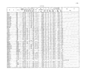
32-2 AMD o~70 | 450 of 450] 100) 45455 150/30] 0.8] 20| 6] 0.45/21 2.4/0.4] 12 | An27 324-2006 AND o~70 | 200 of mo] so) 45~55 100725] 0.8| 20] 6] 0.45/21 2.4/0.4| 12 | n2732A-250C AMD o~70 | 250 [oj wo! so) 45~55 1o025| 08] 20] 6| 0.45/21 2.4/0.4) 12 | An2732A-206 AMD o~70 | 200 of 70] 60] 45~55 100/25 { 0. = 0. 45/2.1 24/0.4| 12 _ An2732A-300C AND o~70 | 300 o[ iso) 130, 45~5.5 10/25 0.8] 20] 6[ 0.45/21 2.4/0.4 12 An27324-30C AMD o~70 | 300 of iso} 10. 45455 woes{ 08] 20] 6| 045/21 2.4/0.4] 12 | An2792A-45D AND a~70 | 450 of iso] 130[ 45455 1072s; 0.8] 20] 6| 0.45/21 2.4/0.4] 12 _| An2732A-ADC AND t~70 | 450 a| 190] 190) 4.5~5.5 100/25] oa] 20, 6{ 0.45/21 rl a An2732A-DC AMD o~70 [250 of tof so; 45~5.5 wov25{ as] 20] 6{ 045/21 247.4{ 12 | AmZ7I2APC AMD o~70 [250 of] wo] sof 45~5.5 100/25] 08] 20/ 6] 0.45/21 24/04] 12 62732 INTEL o~70] 450} 120[ 0 100] 4. 75~5. 25 150/30, 08) 20] 6| 0.45/21 2.4/-|_12| Ce c2732-6 INTEL 0 100 | 4. 75~5. 25 150/30| a8] 20] 6| 0.45/21 2.4/-| 12{ Ce | C2732A INTEL t~
 2 Pages, 77 KB, Scan
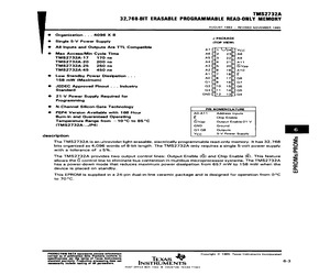
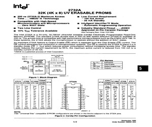
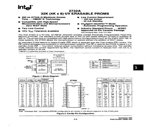
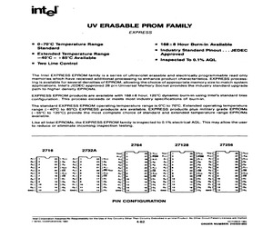
2732A-20 200 ns TMS2732A-25 250 ns TMS2732A-45 450 ns @ Low Standby Power Dissipation . . . 158 mW (Maximum) @ JEDEC Approved Pinout . . . Industry Standard @ 21-V Power Supply Required for Programming AUGUST 1983 REVISED NOVEMBER 19385 J PACKAGE (TOP VIEW) 471 U2 vec a6 []2 73H ae 453 220] a9 aoe aitjait a3 (5 79H Sivee A2[}s is{} aro aifi7 islje& aos 17[C)a8 ai[j9 16[Ja7 o2[i0 15[ Jas o3(]11 140 05 Gno(ji2 13f} a4 @ N-Channel Silicon-Gate Technology PIN NOMENCLATURE @ PEP4 Version Available with 168 Hour AO-A11 Burn-in and Guaranteed Operating E Temperature Range from 10C to 85C G/Vpp (TMS2732A-__JP4) GND 21-08 description Vee Address Inputs Chip Enable Output Enable/21 V Ground Outputs 5-V Power Supply The TMS2732A is an ultraviolet light-erasable, electrically programmable read-only memory. It has 32,768 bits organized as 4,096 words of 8-bit length. The TMS2732A only requires a single 5-volt power supply with a tolerance of +5%. The TMS2732A provides two output control lines: Output Enable (
 7 Pages, 157 KB, Scan
s above those indicated in the operational sections of this specification is not implied. Exposure to absolute maximum rating con- ditions for extended periods may affect device reliability. D.C. AND A.C. OPERATING CONDITIONS DURING READ 2732A/A-2/A-3/A-4 2732A-20/A-25/A-30 Operating Temperature Range oc-70C orc-70C Voc Power Supply SV + 5% 5V + 10% READ OPERATION D.C. CHARACTERISTICS Symbol Parameter Min. Tet Max. Units Conditions he Input Load Current 10 HA | Vin = 5.5V lLo Output Leakage Current 10 uA | Vout = 5.5V lecr Vec Current (Standby) 35 mA | CE=Viy, OF= Vip loce Voc Current (Active) 100 mA | OE =CE=Vy_ Vit Input Low Voltage ~0.1 0.8 v Vin input High Voltage 2.0 Voc +1 Vv Vor Output Low Voltage 0.45 Vi] lop = 2.1 mA Vou Output High Voitage 2.4 Vv lon = 400 pA Vpp" Vpp Read Voltage 3.8 Veco V_ | Vog=5.0V+ 0.25V A.C. CHARACTERISTICS 2732A-2 2732A 2732A-3 | 27304-4 2732A-20 | 2732A-25 | 2732A-30 Test Symbol Parameter Min. | Max.| Min.| Max. | Min. | Max. | Min.| Max. | Units|
 7 Pages, 257 KB, Scan
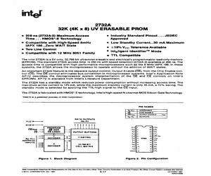
2732A-20 200 ns TMS2732A-25 250 ns TMS2732A-45 450 ns All Inputs/Outputs Fuly TTL Compatible @ Low Standby Power Dissipation .. . 158 mW (Maximum) @ JEDEC Approved Pinout... Standard @ 21-V Power Supply Required for Programming @ N-Channel Silicon-Gate Technology @ PEP4 Version Available with 168 Hour Burn-in, and Extended Guaranteed Operating Temperature Range from 10C to 85C (TMS2732A-_ _JP4) description Industry AUGUST 1983REVISED FEBRUARY 1988 J PACKAGE (TOP VIEW) A7(]1 V2aQ vec A6qj2 230s as(j3 22Djag A4f]4 21f}ait A3(]5 20f]G/vpp A2(]6 Bia AiQ77 18DE Aot}s 1708 aifj9 16fja7 Q2[j10 15)[Ja6 o3{]11 14705 GND (J12 130} 04 PIN NOMENCLATURE A0-A11 E Gvpp GND Q1-08 Vec Address Inputs Chip Enable Output Enable/21 V Ground Outputs 5-V Power Supply EPROMs/PROMs/EEPROMs The TMS2732A is an ultraviolet light-erasable, electrically programmable read-only memory. it has 32,768 bits organized as 4,096 words of 8-bit length. The TMS2732A only requires a single 5-volt power supply with a tolerance of +5%. Th
 7 Pages, 189 KB, Scan
 OE = Vit 70 125 mA Vit Input low voltage -0.1 +0.8 Vv ViH Input high voltage 2.0 Vec+ 1 Vv VoL Output Low voltage lo. = 2.1 mA 0.45 Vv Vou Output high voltage loH = -400 pA 2.4 Vv AC CHARACTERISTICS 2732A-2 2732A 2732A-3 2732A-4 Symbol Parameter Covttion 2732A-20 2732A-25 2732A-30 2732A-45 Unit Min | Max | Min | Max | Min | Max | Min | Max taco | Address to Output | CE_GE=Vvi. 200 250 300 450 | ns Delay tce CE to Output delay | OE=Vit 200 250 300 450 ns tor OE to Output Delay! CE=ViL 100 100 150 150 ns tor) | OF High to Output SEV se | o 6 o | 130 | 0 | 130 ns Output hold from__ address, CE or OE | ae_ae_ toH | Whichever occured | CE=OE=Vin 0 0 0 ns first CAPACITANCE (Tams = 25C, f = 1 MHz) Symbol! Parameter Test Condition Min Typ Max Unit Input Capacitance except _ Cin OEVer Vin = OV 4 6 pF Cine OE/Vpe Input Capacitance Vin = OV , 20 pF Court Output Capacitance Vout = OV 8 12 pF NOTES : 1. Vcc must be applied simultaneously or before Ver and removed simultaneously or after Vpp. 2. Vpp may be co
 7 Pages, 277 KB, Scan
2732A-20 200 ns TMS2732A-25 250 ns TMS2732A-45 450 ns All Inputs/Outputs Fuly TTL Compatible @ Low Standby Power Dissipation .. . 158 mW (Maximum) @ JEDEC Approved Pinout... Standard @ 21-V Power Supply Required for Programming @ N-Channel Silicon-Gate Technology @ PEP4 Version Available with 168 Hour Burn-in, and Extended Guaranteed Operating Temperature Range from 10C to 85C (TMS2732A-_ _JP4) description Industry AUGUST 1983REVISED FEBRUARY 1988 J PACKAGE (TOP VIEW) A7(]1 V2aQ vec A6qj2 230s as(j3 22Djag A4f]4 21f}ait A3(]5 20f]G/vpp A2(]6 Bia AiQ77 18DE Aot}s 1708 aifj9 16fja7 Q2[j10 15)[Ja6 o3{]11 14705 GND (J12 130} 04 PIN NOMENCLATURE A0-A11 E Gvpp GND Q1-08 Vec Address Inputs Chip Enable Output Enable/21 V Ground Outputs 5-V Power Supply EPROMs/PROMs/EEPROMs The TMS2732A is an ultraviolet light-erasable, electrically programmable read-only memory. it has 32,768 bits organized as 4,096 words of 8-bit length. The TMS2732A only requires a single 5-volt power supply with a tolerance of +5%. Th
 12 Pages, 852 KB, Scan
0 mA OE = CE = Vit Vit Input Low Voltage 0.1 0.8 Vv Vin Input High Voltage 2.0 Voc + 1 Vv VoL Output Low Voltage 0.45 Vv lop = 2.1MA VoH Output High Voltage 2.4 Vv lon = 400 pA A.C. CHARACTERISTICS 0C < Ta < 70C Versions Voc +5% 2732A-2 2732A Test Vec 10% 2732A-20 2732A-25 Units Conditions Symbol Parameter Min Max | Min | Max tacc Address to Output Delay 200 250 ns CE = OF = Vi toe CE to Output Delay - 200 250 ns OE = ViL toe OE/Vpp to Output Delay 70 100 ns CE = Vit tor (4) OE/Vpp High to Output Float 60 60 ns CE = Vit tou{4) Output Hold from Addresses, 0 ns CE = OE = Vi CE or OE/Vpp, Whichever Occurred First NOTES: 1. Voc must be applied simultaneously or before OE/Vpp and removed simultaneously or after OE/Vpp. 2. The maximum current value is with outputs Og to O7 unloaded. 3. Typical values are for Ta = 25C and nominal supply voltages. 4. This parameter is only sampled and is not 100% tested. Output Float is defined as the point where data is no longer drivensee timing diagram.intel 2732A CAP
 9 Pages, 316 KB, Scan
hese one-time programmable PLCC EPROMs for your next project that requires memory. These devices are low power and take up less PC board space than their DIP counterparts. Part # Speed TMS2516 450ns 2716-1 350ns 2716B 450ns 2732A-450 450ns 2732A-250 250ns 2732A-200 200ns 2764A-300 300ns 2764A-200 200ns 27C64A-200 200ns 27C64A-150 150ns 7C261-35 35ns 27128A-250 250ns 27128A-150 150ns 27C128A-120 120ns 7C254-45 45ns 27256-200 200ns 27C256-200 200ns 27C256-150 150ns 27C256-100 100ns 27C256-90 90ns 27C256-55 55ns 7C271-45 45ns 27512-250 250ns 27512-200 200ns 27C512-150 150ns 27C512-120 120ns 27C512-100 100ns 27C512-70 70ns 27C1024-200 200ns 27C1024-120 120ns 27C101-200 200ns 27C101-150 150ns 27C101-100 100ns 27C101-70 70ns 27C101-45 45ns 27C1000-120 120ns 27C201-150 150ns 27C201-100 100ns 27C4096-100 100ns M27C4002-10C1 100ns 27C401-120 120ns 27C401-100 100ns 27C401-80 80ns 27C800-100 100ns 27C801-100 100ns 27C801-90 90ns Org Pins VPP Each Qty Bulk Price 2k x 8 24 5 $3.25 15 $3.00 2k x 8 24 25 $6.99
 10 Pages, 1659 KB, Original
A8 270ZA05 270ZS05 270ZT05 271 HARR HARR HARR HARR HARR HARR HARR HARR HARR NSC 0.400 0.350 0.420 2.660 3 660 2.350 0.300 0.340 0.340 0.600 M 0.400 0.350 0.420 2.660 3.660 2,350 0.300 0.340 0.340 0.600 AY TIVIS TIVIS TIVIS TIVIS TIVIS HLNP HLNP EISN IC IC 2732A-20JL 2732A-25.1L 2732A-30JL 2732A-35JL 2732A-45JL 2735 2735#S02 274 T/R 274-10 274-20 TI TI TI TI TI HP HP PHIL TI TI 7.220 6.660 6.110 5.770 5550 2.240 A 2450 A 0.548 N 376.000 26.000 7.220 5.430 AC 6.660 5.010 AC 6.110 4.590 AC 5.770 4.340 AC 5.550 4,180 AC 1,920 ID 1.760 AT 2.090 D 1.920 AT 0.480 BC 37E000 376.000 260.000 260.000 5.040 AL 4.650 AL 4.260 AL 4.030 AL 3.880 AL 1 .660BC 1.800BC HCMS HCIV1S MPS HCMS HCMS NM HCIVIS NM FSA FSA 2710 2711 2711 2712 2713 2713 2714 2716 2719M 271912 HP HP NSC HP HP NSC HP NSC NSC NSC 35.840 A 37.950 A 0.170 N 37.950 A 37.950 A 0.170 N 37.950 A 0.170 N 4.380 I 2.820 I 33.090 Z 35.030 Z 0.130 BC 35.030 Z 35.030 Z 0.110 BC 35.030 Z 0.110 BC 3.370 AL 2.170 AL 30.720 AE 28.670 AL 32530 AE 30.360 AL 0.1
 1 Pages, 38 KB, Original
 mA OE = CE = Vit Vit Input Low Voltage -0.1 0.8 v Vin Input High Voltage 2.0 Voc + 1 Vv VoL Output Low Voitage 0.45 Vv lo. = 2.1 mA Vou Output High Voltage 2.4 Vv lon = 400 nA A.C. CHARACTERISTICS oc < Ta < 70C Versions Voc +5% 2732A-2 2732A Test Voc 10% 2732A-20 2732A-25 Units Conditions Symbol Parameter Min | Max | Min | Max tacc Address to Output Delay 200 250 ns CE = OF = Vi tcE CE to Output Delay 200 250 ns OE = ViL toe OE/Vpp to Output Delay 70 100 ns CE = Vit tori) OE/Vpp High to Output Float 60 60 ns CE = Vit ton(4) Output Hold from Addresses, ns CE = OE = ViL CE or OE/Vpp, Whichever Occurred First NOTES: 1. Voc must be applied simultaneously or before OE/Vpp and removed simultaneously or after GE/Vpp. 2. The maximum current value is with outputs Og to O7 unloaded. 3. Typical values are for Ta = 25C and nominal supply voltages. 4. This parameter is only sampled and is not 100% tested. Output Float is defined as the point where data is no longer drivensee timing diagram.intel 2732A CAPACI
 9 Pages, 302 KB, Scan
716 2048x8 . 450 5V + 5% -40 to 85 168+8 TD2716 2048x8 450 5V = 5% -40 to 85 NONE QD2732A-2 4096x8 200 5V + 5% 0 to 70 168+8 QD2732A 4096x8 250 5V + 5% 0 to 70 168+8 QD2732A-3 . 4096x8 300 5V + 5% 0 to 70 1688 Q0D2732A-4 4096x8 450 5V + 5% 0 to 70 168+8 QD2732A-20 4096x8 200 5V + 10% - Qto 70 1688 QD2732A-25 4096x8 250 SV + 10% 0 to 70 168+8 QD2732A-30 4096x8 300 5V + 10% 0 to 70 168+8 LD2732A 4096x8 250 5V = 5% ~40 to 85 168+8 LD2732A-4 4096x8 450 5V + 5% ~40 to 85 168+8 L02732A-25 4096x8 250 5V + 10% - 40 to 85 168+8 LD2732A-45 4096x8 450 5V + 10% -40 to 85 168+8 1D2732A 4096x8 250 5V + 5% -40 to 85 NONE TO2732A-4 4096x8 450 5V + 5% -40 to 85 NONE T02732A-25 4096x8 250 5V + 10% -40 to 85 NONE TD2732A-45 4096x8 450 5V + 10% ~40 to 85 NONE QD2764-2 8192x8 200 5V + 5% 0 to 70 168+8 Q02764 8192x8 250 5V = 5% 0 to 70 16828 QD2764-3 8192x8 300 5V + 5% 0 to 70 168+8 QD2764-4 8192x8 450 5V + 5% 0 to 70 168+8 QD2764-25 8192x8 250 5V + 10% 0 to 70 168+8 QD2764-30 8192x8 300 5V + 10% 0 to 70 168+8 QD2764-
 4 Pages, 116 KB, Scan
28 6500 +5 HN613128 16384 X 8 HN61256 32768x 8 65536X 4 3500 7.5m HN613256 32768 8 250 5p/75m 1M-bit HN62301** 131072 X 8 350 5m/60m 28 16k-bit HN462716 2048 X 8 450 0.555 24 X 250 28 HN462532 0.858 450 HN462732 32k-bit HN482732A-25 u. V. Erasable & - HN482732A-20 4096 X 8 NMOS - - 128k-bit +5 8192 X 8 300 - HN482764-4 450 HN4827128-25** 250 NMOS 16384 X 8 300 - HN4827128-45** Electrically Erasable * ** *** 16k-bit HN48016 0.555 28 0.554 28 0.16 24 450 NMOS 16384 X 8 350 +5 P FP * * * * * * * * * * * * * * * * * * * ment Page 292 294 296 298 * 300 * * 302 304 306 * 250 - * * * * * * * * 0.788 300 HN482764-3 HN4827128-30** 24 250 - HN482764 64k-bit 0.788 200 HN482732A-30 Electrically G 5p/0.05 CMOS 256k-bit C 28 250 I--8192 X 8 250 I--250 HN61366 Mask Time (word) Xbit HN61364 64k-bit Acces~ zation Process 2716 310 TMS2532 314 2732 318 2732A-2 325 2732A 325 2732A-3 325 2764 328 2764-3 328 328 332 332 332 * 336 Under development Preliminary The package codes of C, G, P and FP are applied to the pack
 447 Pages, 126941 KB, Original


