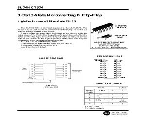
s, data may be stored even when the outputs are not enabled. * TTL/NMOS Compatible Input Levels * Outputs Directly Interface to CMOS, NMOS, and TTL * Operating Voltage Range: 4.5 to 5.5 V * Low Input Current: 1.0 A ORDERING INFORMATION SL74HCT574N Plastic SL74HCT574D SOIC TA = -55 to 125 C for all packages PIN ASSIGNMENT LOGIC DIAGRAM FUNCTION TABLE PIN 20=VCC PIN 10 = GND Inputs Output Enable Output D Q L H H L L L X no change X Z L H Clock L,H, X X = don't care Z = high impedance SLS System Logic Semiconductor SL74HCT574 MAXIMUM RATINGS * Symbol Parameter Value Unit -0.5 to +7.0 V VCC DC Supply Voltage (Referenced to GND) VIN DC Input Voltage (Referenced to GND) -1.5 to VCC +1.5 V DC Output Voltage (Referenced to GND) -0.5 to VCC +0.5 V DC Input Current, per Pin 20 mA DC Output Current, per Pin 35 mA ICC DC Supply Current, VCC and GND Pins 75 mA PD Power Dissipation in Still Air, Plastic DIP+ SOIC Package+ 750 500 mW -65 to +150 C 260 C VOUT IIN IOUT Tstg Storage Temperature TL Lead Temperature
 6 Pages, 52 KB, Original


