aces JVC BN-V428U * 7.2Volt 2800mAh (4hr.) * NoMEM Lithium-Ion * 3 Year Warranty Dimensions: 2-1/8 x 1-1/2 x 2-1/8 Description: * Replaces JVC BN-V114U * 7.2Volt 1550mAh (2.25hr.) * NoMEM Lithium-Ion * 3 Year Warranty Dimensions: 1-15/16 x 2-11/16 x 1/2 LIJ507 LIJ207 Description: * Replaces JVC BN-V507U * 7.2Volt 820mAh (1hr.) * NoMEM Lithium-Ion * 3 Year Warranty Dimensions: 2 x 2-1/2 x 3/8 Description: * Replaces JVC BN-V207U * 7.2Volt 1150mAh (1hr.) * NoMEM Lithium-Ion * 3 Year Warranty Dimensions: 2-7/8 x 1-9/16 x 3/4 For the most up-to-date information and cross reference listings, go to www.lenmar.com or www.BatteryCentral.com U.S. Phone: 800.424.2703 or 805.384.9600 Fax: 805.384.9693 - International Phone: 852.2519.9728 Fax: 852.2519.0122 25 Camcorder Battery Picture Index & Specifications Model # Information Model # LIJ514 LIP14 Description: * Replaces JVC BN-V514U * 7.2Volt 1850mAh (2.5hr.) * NoMEM Lithium-Ion * 3 Year Warranty Dimensions: 2 x 2-1/2 x 1 Description: * Replaces Panasonic
 106 Pages, 4800 KB, Original
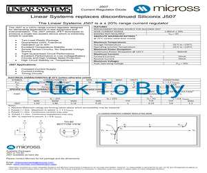
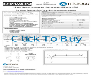
J507 Current Regulator Diode Linear Systems replaces discontinued Siliconix J507 The Linear Systems J507 is a 20% range current regulator The J507 is a 20% range current regulator designed for demanding applications in test equipment and instrumentation. The J507 utilizes JFET techniques to produce a single two-leaded device which is extremely simple to operate. * * * * * * * * Two-Lead Plastic Package Guaranteed 20% Tolerance Operation up to 50V Excellent Temperature Stability Simple Series Circuitry, No Separate Voltage Source Tight Guaranteed Circuit Performance Excellent Performance in Low-Voltage/Battery Circuits and High-Voltage Spike Protection High Circuit Stability vs. Temperature. J507 Applications: * * * FEATURES REPLACEMENTSECONDSOURCEFORSILICONIXJ507 WIDECURRENTRANGE 1.80mA20% BIASINGNOTREQUIRED VGS=0V ABSOLUTEMAXIMUMRATINGS1 @25C(unlessotherwisenoted) MaximumTemperatures StorageTemperature OperatingJunctio
 1 Pages, 352 KB, Original
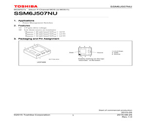
J507NU MOSFETs Silicon P-Channel MOS (U-MOS) SSM6J507NU 1. Applications * Power Management Switches 2. Features (1) 4 V gate drive voltage. (2) Low drain-source on-resistance : RDS(ON) = 20 m (max) (@VGS = -10 V) RDS(ON) = 28 m (max) (@VGS = -4.5 V) RDS(ON) = 32 m (max) (@VGS = -4.0 V) 3. Packaging and Pin Assignment 1.2.5.6 Drain 3. Gate 4. Source UDFN6B Start of commercial production (c)2015 Toshiba Corporation 1 2015-05 2015-11-10 Rev.2.0 SSM6J507NU 4. Absolute Maximum Ratings (Note) (Unless otherwise specified, Ta = 25 ) Characteristics Symbol Rating Unit V Drain-source voltage VDSS -30 Gate-source voltage VGSS -25 / +20 Drain current (DC) Drain current (pulsed) Power dissipation Power dissipation (t 10 s) (Note 1) ID -10 (Note 1), (Note 2) IDP -30 A (Note 3) PD 1.25 W (Note 3) PD 2.5 W Channel temperature Tch 150 Storage temperature Tstg -55 to 150 Note: Using continuously under heavy loads (e.g. the application of high temperature/current/voltage and the significan
 9 Pages, 241 KB, Original
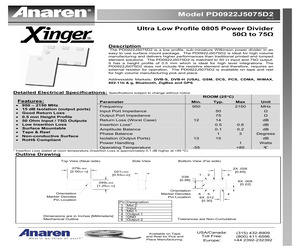
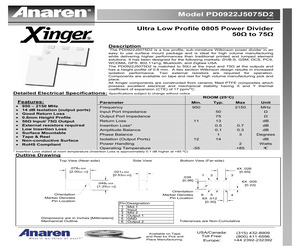
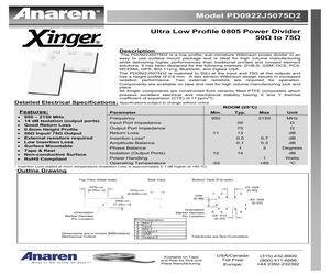
J5075D2 Rev B Ultra Low Profile 0805 Power Divider 50 to 75 Description The PD0922J5075D2 is a low profile, sub-miniature Wilkinson power divider in an easy to use surface mount package. The PD0922J5075D2 is ideal for high volume manufacturing and delivers higher performances than traditional printed and lumped element solutions. The PD0922J5075D2 is matched to 50 input and 75 output. It has a height profile of 0.5 mm which is ideal for high level integrations. The PD0922J5075D2 does not include the resistive element and therefore, requires an external resistor for operation. The PD0922J5075D2 is available on tape and reel for high volume manufacturing pick and place. Addressable Markets: DVB-S, DVB-H (USA), GSM, DCS, PCS, CDMA, WiMAX, 802.11b & g, Bluetooth, ZigBee and GPS Detailed Electrical Specifications: Specifications subject to change without notice. ROOM (25C) Features: * * * * * * * * * * 950 - 2150 MHz 15 dB Isolation (out
 6 Pages, 230 KB, Original
 U8 U9 U13 U12 U11 U21 U15 U14 U16 U19 U17 J10 U22 U23 U25 U20 U26 J11 U27 U31 U29 U28 J12 U30 SW2 21 7233 N/B MAINTENANCE 2. Definition & Location Major Components/connectors (Side B) PJ500: Power Jack. J506: PCMCIA CONN J500: PS/2 Key-Board/ Mouse CONN. J507: CO-ROM CONN J501: VGA CONN. J508: 144 PINS SODIMM Socket. J502: Serial Port. J509: Battery Connector. J503: Parallel Port. SW500: Power Switch. J504: FAX Modem CONN U501: uPGAII CPU. U504:IR LANs U508: H8/F3434 Key-Board Controller. PS/2 Key-Board/ Mouse CONN J1: Audio Output; J2: MIC EXT Power Jack Parallel Port VGA CONN USB Port Serial Port 22 7233 N/B MAINTENANCE 2. Definition & Location Major Components (Side B) J503 J500 J502 J501 PJ500 SW500 U501 PU504 J504 J506 J508 U504 J507 U508 J509 J509 23 7233 N/B MAINTENANCE 3. Pin Descriptions of Major Componts 3.1 Intel PGAII CPU Processor-1 Alphabetical Signal Reference Signal Name A[35:3]# A20M# ADS# AERR# AP[1:0]# BCLK I/O Signal Description I/O The A[35:3]# (Address) signals
 121 Pages, 1118 KB, Original
J507NU MOSFETs Silicon P-Channel MOS (U-MOS) SSM6J507NU 1. Applications * Power Management Switches 2. Features (1) 4 V gate drive voltage. (2) Low drain-source on-resistance : RDS(ON) = 20 m (max) (@VGS = -10 V) RDS(ON) = 28 m (max) (@VGS = -4.5 V) RDS(ON) = 32 m (max) (@VGS = -4.0 V) 3. Packaging and Pin Assignment 1.2.5.6 Drain 3. Gate 4. Source UDFN6B Start of commercial production (c)2015 Toshiba Corporation 1 2015-05 2015-08-25 Rev.1.0 SSM6J507NU 4. Absolute Maximum Ratings (Note) (Unless otherwise specified, Ta = 25 ) Characteristics Symbol Rating Unit V Drain-source voltage VDSS -30 Gate-source voltage VGSS -25 / +20 Drain current (DC) Drain current (pulsed) Power dissipation Power dissipation (t 10 s) (Note 1) ID -10 (Note 1), (Note 2) IDP -30 A (Note 3) PD 1.25 W (Note 3) PD 2.5 W Channel temperature Tch 150 Storage temperature Tstg -55 to 150 Note: Using continuously under heavy loads (e.g. the application of high temperature/current/voltage and the significan
 10 Pages, 243 KB, Original
J507797 TECHNICAL MANUAL Service And Parts S-21E Wire Feed Equipment A WARNING Use MILLER Testing Booklet (Part No. 150 853) when servicing this unit. SERVICING can be hazardous. * Have all service procedures performed only by qualified persons following standard safety practices. U coverjml -- For help, call Factory Service Department: 414-735-4505 SB-124 467 ~U~r Use only genuine MILLER replacement parts. FAX: 14-735-4136 U L................J (c) 1996 MILLER Electric Mfg. Co. Or write to: MILLER Electric Mfg. Co. RO. Box 1079 Appleton, WI 54912 USA PRINTED IN USA OM-1571B TABLE OF CONTENTS Section No. SECTION 1 1-1. 1-2. 1-3. - Page No. SAFETY PRECAUTIONS AND SIGNAL WORDS General Information And Safety Safety Alert Symbol And Signal Words Safety Precautions 1 1 1 SECTION 2- SHIPPING AND STORAGE 2-1. 2-2. Preparation For Reshipment Storage 2 2 SECTION 3-- SPECIFICATIONS 3-1. Description 3 SECTION 4- INSTALLATION OR RELOCATION 4-1. 4-2. 4-3. 4-4. 4-5. 4-6. 4-7. 4-8. 4-9. 4-10. Location Drive Roll
 48 Pages, 2847 KB, Original
ail Button 46 M762 N/B Maintenance 3. Definition & Location of Connectors / Switches 3.1 Mother Board - B J502 : 144 pin SODIMM Slot J503 : D/D Board Connector. J502 J503 J504 : PCMCIA Card Slot J505 : USB Connector J506 : MDC/LAN Transfer Board Connector J507 : CD-ROM Transfer Board Connector J508 : CMOS Battery Connector J504 J509 : IEEE1394 Connector J505 J506 J507 J508 J509 VR501: Volume Control VR501 47 M762 N/B Maintenance 3. Definition & Location of Connectors / Switches 3.2 Daughter Board J16: MDC Jump Wire Connector JP1 : MDC Jump Wire Connector J17 : RJ-11 Phone Jack for Internal Modem JP3 : MDC/LAN Transfer Board to M/B Connector 2 J18 : MDC/LAN Transfer Board to M/B Connector 1 J19 : RJ45 Connector MDC/LAN Transfer Board J18 J19 JP1 J17 JP3 J16 48 M762 N/B Maintenance 3. Definition & Location of Connectors / Switches 3.3 Charger Board J501 : D/D Board Connector DC to DC board (side A) J1 : External VGA Connector J2 : Inverter Board Connector J501 J3 : USB Port J4 : FAN Co
 153 Pages, 7146 KB, Original
J5075D2 Rev D Ultra Low Profile 0805 Power Divider 50 to 75 Description The PD0922J5075D2 is a low profile, sub-miniature Wilkinson power divider in an easy to use surface mount package and is ideal for high volume manufacturing while delivering higher performances than traditional printed and lumped element solutions. It has been designed for the following markets: DVB-S, GSM, DCS, PCS, WCDMA, GPS, 802.11a+g, Bluetooth, and Zigbee USA. The PD0922J5075D2 is matched to 50 at the input and 75 at the outputs and has a height profile of 0.8 mm. A two section Wilkinson design results in increased isolation performance. Two external resistors are required for operation. Components are available on tape and reel for high volume manufacturing pick and place. All Xinger components are constructed from ceramic filled PTFE composites which possess excellent electrical and mechanical stability having X and Y thermal coefficient of expansion (CTE) of 17 ppm/oC. Detailed Electrical Sp
 6 Pages, 229 KB, Original
J5075D2 Rev C Ultra Low Profile 0805 Power Divider 50 to 75 Description The PD0922J5075D2 is a low profile, sub-miniature Wilkinson power divider in an easy to use surface mount package and is ideal for high volume manufacturing while delivering higher performances than traditional printed and lumped element solutions. It has been designed for the following markets: DVB-S, GSM, DCS, PCS, WCDMA, GPS, 802.11a+g, Bluetooth, and Zigbee USA. The PD0922J5075D2 is matched to 50 at the input and 75 at the outputs and has a height profile of 0.8 mm. A two section Wilkinson design results in increased isolation performance. Two external resistors are required for operation. Components are available on tape and reel for high volume manufacturing pick and place. All Xinger components are constructed from ceramic filled PTFE composites which possess excellent electrical and mechanical stability having X and Y thermal coefficient of expansion (CTE) of 17 ppm/oC. Detailed Electrical Sp
 6 Pages, 240 KB, Original
: J501 Ethernet Interrupt Signal Configuration ........................ 33 Table 16: J503 Ethernet Ready Signal Configuration ............................ 34 Table 17: J504 Ethernet LAN_IRQ Pull-up Configuration................... 34 Table 18: J505, J506, J507 Ethernet EEPROM Configuration ............. 34 Table 19: J508 Ethernet EEPROM Enable Configuration ..................... 35 Table 20: J509 Ethernet nLNK Pin Configuration ................................. 35 Table 21: J600, J601 CAN Transceiver Activation ................................ 36 Table 22: J616 CAN Transceiver Supply Configuration........................ 37 Table 23: J602, J603, J604 and J605 CAN Interface Configuration ...... 38 Table 24: J606 EEPROM Write Protection ............................................ 38 Table 25: J607 Watchdog Configuration................................................ 39 Table 26: J608, J609, J610 I2C Interface Configuration......................... 40 Table 27: J611, J612, J613, J614 SPI Interface
 144 Pages, 1931 KB, Original
J507 Current Regulator Diode Linear Systems replaces discontinued Siliconix J507 The Linear Systems LSJ507 is a 20% range current regulator The LSJ507 is a 20% range current regulator designed for demanding applications in test equipment and instrumentation. The LSJ507 utilizes JFET techniques to produce a single two-leaded device which is extremely simple to operate. * * * * * * * * Two-Lead Plastic Package Guaranteed 20% Tolerance Operation up to 50V Excellent Temperature Stability Simple Series Circuitry, No Separate Voltage Source Tight Guaranteed Circuit Performance Excellent Performance in Low-Voltage/Battery Circuits and High-Voltage Spike Protection High Circuit Stability vs. Temperature. LSJ507 Applications: * * * FEATURES REPLACEMENT SECOND SOURCE FOR SILICONIX J507 WIDE CURRENT RANGE BIASING NOT REQUIRED ABSOLUTE MAXIMUM RATINGS 1 @ 25C (unless otherwise noted) Maximum Temperatures Storage Temperature Operati
 1 Pages, 356 KB, Original
1 14.1" 0 0 0 1 Unipac UP141X01-2 14.1" 0 0 1 0 Hyundai 14X13-101 14.1" 1 0 0 0 Hyundai HT15X31 15" 1 0 0 1 Hitachi TX38D85VC1CAA 15" 77 7521Plus / N N/B MAINTENANCE 3. Definition & Location Of Connectors / Switches 3.3 Mother Board-B PJ501 J502 J508 J505 J507 J506 J504 J501 J503 U501 U502 J509 BT501 J510 J511 U503 VR501 J506 J512 J513 J514 J516 J515 PJ501: Power jack ( AC adapter). J507: VGA Connector. J516 :HDD/FDD Connector. J502 : PS2 Mouse/keyboard. J508: USB connector. J512: CD-ROM drive connector. J503: Line in Jack. J509: Phone Jack Connector. J514: Charger & Touch-Pad connector. J504: RJ45 LAN connect. J510: Line Out with APDIF. J515: Touch-Pad button connector. J505: Parallel Port. J511: MDC MODEM transfer BD connector. BT501: CMOS Battery connector. J506: PCMCIA card socket. J513: CPU FAN Connector. VR501: Volume control VR. U503: FC-PGA Socket 370 CPU Slot. 78 7521Plus / N N/B MAINTENANCE 3. Definition & Location Of Connectors / Switches 3.4 Daughter Board MDC/LAN transfe
 180 Pages, 5745 KB, Original
Board (Side A) - 1 PJ501 : AC Power Jack J509 J506 J501 : Battery Connector J518 J519 J502 : Fan Connector J501 J520 J514 J503 : Left Internal Speaker Jack J504 : Inverter Board Connector J513 J516 J511 J505 : LCD Connector J506 : DC to DC Board Connector J507 : External VGA Connector J504 J517 J509 SW501 J508 : S-Video Connector J505 J509 : Secondary EIDE Connector J510 J515 J512 J508 J503 J507 J502 PJ501 74 J510 : USB Port Connector ------ To next page ------ Prestigio Nobile 141 TECHNICAL SERVICE MANUAL 3. Definition & Location of Connectors / Switches 3.1 Main Board (Side A) - 2 ------ Continued to previous page -----J511 : RTC Battery Connector J509 J506 J512 : USB Port Connector J518 J519 J501 J520 J513, J514 : DDR SO-DIMM Module Socket J514 J515 : RJ-45 Connector J516 : Card Reader Socket J513 J516 J511 J517 : PCMCIA Card Socket J518 : Line Out Jack J519 : External Microphone Jack J504 J517 J509 SW501 J520 : Mini PCI Socket J505 SW501 : Audio DJ Button J510 J515 J512 J508 J503
 184 Pages, 33283 KB, Original
Board (Side A) - 1 PJ501 : AC Power Jack J509 J506 J501 : Battery Connector J518 J519 J502 : Fan Connector J501 J520 J514 J503 : Left Internal Speaker Jack J504 : Inverter Board Connector J513 J516 J511 J505 : LCD Connector J506 : DC to DC Board Connector J507 : External VGA Connector J504 J508 : S-Video Connector J505 J517 J509 J509 : Secondary EIDE Connector J510 J515 SW501 J512 J508 J503 J507 J502 PJ501 J510 : USB Port Connector ------ To next page ------ 74 8080 N/B Maintenance 3. Definition & Location of Connectors / Switches 3.1 Main Board (Side A) - 2 ------ Continued to previous page -----J511 : RTC Battery Connector J509 J506 J512 : USB Port Connector J518 J519 J513, J514 : DDR SO-DIMM Module Socket J501 J520 J514 J515 : RJ-45 Connector J516 : Card Reader Socket J513 J516 J511 J517 : PCMCIA Card Socket J518 : Line Out Jack J519 : External Microphone Jack J504 J520 : Mini PCI Socket J505 J517 J509 SW501 : Audio DJ Button J510 J515 SW501 J512 J508 J503 J507 J502 P
 184 Pages, 32799 KB, Original


