ry Table 12. Revision history Document ID Release date Data sheet status Change notice Supersedes HEF4070B v.5 20151216 Product data sheet - HEF4070B v.4 Modifications: HEF4070B v.4 Modifications: HEF4070B_CNV v.3 HEF4070B Product data sheet * Type number HEF4070BP (SOT27-1) removed. 20140327 Product data sheet - HEF4070B_CNV v.3 * The format of this data sheet has been redesigned to comply with the new identity guidelines of NXP Semiconductors. * Legal texts have been adapted to the new company name where appropriate. 19950101 Product specification - All information provided in this document is subject to legal disclaimers. Rev. 5 -- 16 December 2015 - (c) Nexperia B.V. 2017. All rights reserved 8 of 11 HEF4070B Nexperia Quad 2-input EXCLUSIVE-OR gate 16. Legal information 16.1 Data sheet status Document status[1][2] Product status[3] Definition Objective [short] data sheet Development This document contains data from the objective specification for product development. Preliminary [short] data
 12 Pages, 736 KB, Original
OIC PDIP SOIC SOIC PDIP SOIC SOIC PDIP PDIP SOIC SOIC PDIP Pins 14 14 14 14 14 14 14 14 14 14 14 14 14 14 14 14 16 16 16 14 14 14 14 14 14 14 14 14 14 14 14 14 14 14 16 16 16 16 16 16 16 16 24 24 24 24 24 24 16 16 16 16 16 16 16 16 16 16 16 16 16 16 16 16 HEF4070BPN -- HEF4538BPN 170 Orderable Part Number HEF4070BPN HEF4070BTD HEF4070BTD-T HEF4071BPN HEF4071BT HEF4071BTD HEF4071BTD-T HEF4072BPN HEF4072BTD HEF4072BTD-T HEF4073BPN HEF4073BTD HEF4073BTD-T HEF4075BPN HEF4075BTD HEF4075BTD-T HEF4076BPN HEF4076BTD HEF4076BTD-T HEF4077BPN HEF4077BTD HEF4077BTD-T HEF4078BPN HEF4078BTD HEF4078BTD-T HEF4081BPN HEF4081BTD HEF4081BTD-T HEF4082BPN HEF4082BTD HEF4082BTD-T HEF4093BP HEF4093BTD HEF4093BTD-T HEF4094BPN HEF4502BPN HEF4502BTD HEF4502BTD-T HEF4511BPN HEF4512BPN HEF4512BTD HEF4512BTD-T HEF4514BPN HEF4514BTD HEF4514BTD-T HEF4515BPN HEF4515BTD HEF4515BTD-T HEF4516BPN HEF4517BPN HEF4518BPN HEF4518BTD HEF4518BTD-T HEF4520BPN HEF4520BTD HEF4520BTD-T HEF4521BPN HEF4521BTD HEF4521BTD-T HEF4528B
 441 Pages, 3298 KB, Original
B 74HC4067DB-T 74HC4067D-T 74HC4067N 74HC4067PW 74HC4067PW-T 74HCT4067D 74HCT4067DB 74HCT4067DB-T 74HCT4067D-T 74HCT4067N 74HCT4067PW 74HCT4067PW-T HEF4067BPN HEF4067BTD HEF4067BTD-T HEF4068BPN HEF4068BTD HEF4068BTD-T HEF4069UBPN HEF4069UBTD HEF4069UBTD-T HEF4070BPN HEF4070BTD HEF4070BTD-T HEF4071BPN HEF4071BTD HEF4071BTD-T HEF4072BPN HEF4072BTD HEF4072BTD-T HEF4073BPN HEF4073BTD HEF4073BTD-T 74HC4075D 74HC4075DB 74HC4075DB-T 74HC4075D-T 74HC4075N 74HCT4075D 74HCT4075DB 74HCT4075DB-T 74HCT4075D-T 74HCT4075N 74HCT4075PW 74HCT4075PW-T HEF4075BPN HEF4075BTD HEF4075BTD-T HEF4076BPN HEF4076BTD HEF4076BTD-T HEF4077BPN HEF4077BTD HEF4077BTD-T HEF4078BPN HEF4078BTD HEF4078BTD-T HEF4081BPN HEF4081BTD HEF4081BTD-T HEF4082BPN SN74LV4066ADBR SN74LV4066ADBR SN74LV4066ADR SN74LV4066AN SN74LV4066APW SN74LV4066APWR Not available Not available Not available Not available Not available CD74HC4067M Not available Not available CD74HC4067M96 CD74HC4067E Not available Not available CD74HCT4067M Not available Not avail
 329 Pages, 2106 KB, Original
B 74HC4067DB-T 74HC4067D-T 74HC4067N 74HC4067PW 74HC4067PW-T 74HCT4067D 74HCT4067DB 74HCT4067DB-T 74HCT4067D-T 74HCT4067N 74HCT4067PW 74HCT4067PW-T HEF4067BPN HEF4067BTD HEF4067BTD-T HEF4068BPN HEF4068BTD HEF4068BTD-T HEF4069UBPN HEF4069UBTD HEF4069UBTD-T HEF4070BPN HEF4070BTD HEF4070BTD-T HEF4071BPN HEF4071BTD HEF4071BTD-T HEF4072BPN HEF4072BTD HEF4072BTD-T HEF4073BPN HEF4073BTD HEF4073BTD-T 74HC4075D 74HC4075DB 74HC4075DB-T 74HC4075D-T 74HC4075N 74HCT4075D 74HCT4075DB 74HCT4075DB-T 74HCT4075D-T 74HCT4075N 74HCT4075PW 74HCT4075PW-T HEF4075BPN HEF4075BTD HEF4075BTD-T HEF4076BPN HEF4076BTD HEF4076BTD-T HEF4077BPN HEF4077BTD HEF4077BTD-T HEF4078BPN HEF4078BTD HEF4078BTD-T HEF4081BPN HEF4081BTD HEF4081BTD-T HEF4082BPN SN74LV4066ADBR SN74LV4066ADBR SN74LV4066ADR SN74LV4066AN SN74LV4066APW SN74LV4066APWR Not available Not available Not available Not available Not available CD74HC4067M Not available Not available CD74HC4067M96 CD74HC4067E Not available Not available CD74HCT4067M Not available Not avail
 313 Pages, 2889 KB, Original
4067BM1 HCF4067M013TR HEF4067BPN HEF4067BTD HEF4067BTD-T HCF4068BEY HCF4068BM1 HCF4068M013TR HEF4068BPN HEF4068BTD HEF4068BTD-T HCF4069UBEY HCF4069UBM1 HCF4069UM013TR HCF4069UM013TR HEF4069UBPN HEF4069UBTD HEF4069UBTD-T HCF4070BEY HCF4070BM1 HCF4070M013TR HEF4070BPN HEF4070BTD HEF4070BTD-T MC14070BDR2 HCF4071BEY HCF4071BM1 HCF4071M013TR HEF4071BPN HEF4071BTD HEF4071BTD-T HCF4072BEY HCF4072BM1 HCF4072M013TR HEF4072BPN HEF4072BTD HEF4072BTD-T HCF4073BEY HCF4073BM1 HCF4073M013TR HEF4073BPN HEF4073BTD HEF4073BTD-T 74HC4075D 74HC4075DB 74HC4075DB-T 74HC4075D-T 74HC4075N 74HCT4075D 74HCT4075DB 74HCT4075DB-T 74HCT4075D-T 74HCT4075N 74HCT4075PW Comments -55 to 125C -55 to 125C -40 to 125C -40 to 125C -40 to 125C -40 to 125C -40 to 125C -40 to 125C -40 to 125C -40 to 125C -40 to 125C -40 to 125C -40 to 125C -40 to 125C -40 to 125C -40 to 125C -40 to 125C -40 to 125C -40 to 125C -40 to 125C -40 to 125C -40 to 125C -40 to 125C -40 to 125C -40 to 125C -40 to 125C -40 to 125C Package M Pkg Type SOIC TI Pkg D
 335 Pages, 1395 KB, Original
B 74HC4067DB-T 74HC4067D-T 74HC4067N 74HC4067PW 74HC4067PW-T 74HCT4067D 74HCT4067DB 74HCT4067DB-T 74HCT4067D-T 74HCT4067N 74HCT4067PW 74HCT4067PW-T HEF4067BPN HEF4067BTD HEF4067BTD-T HEF4068BPN HEF4068BTD HEF4068BTD-T HEF4069UBPN HEF4069UBTD HEF4069UBTD-T HEF4070BPN HEF4070BTD HEF4070BTD-T HEF4071BPN HEF4071BTD HEF4071BTD-T HEF4072BPN HEF4072BTD HEF4072BTD-T HEF4073BPN HEF4073BTD HEF4073BTD-T 74HC4075D 74HC4075DB 74HC4075DB-T 74HC4075D-T 74HC4075N 74HCT4075D 74HCT4075DB 74HCT4075DB-T 74HCT4075D-T 74HCT4075N 74HCT4075PW 74HCT4075PW-T HEF4075BPN HEF4075BTD HEF4075BTD-T HEF4076BPN HEF4076BTD HEF4076BTD-T HEF4077BPN HEF4077BTD HEF4077BTD-T HEF4078BPN HEF4078BTD HEF4078BTD-T HEF4081BPN HEF4081BTD HEF4081BTD-T HEF4082BPN SN74LV4066ADBR SN74LV4066ADBR SN74LV4066ADR SN74LV4066AN SN74LV4066APW SN74LV4066APWR Not available Not available Not available Not available Not available CD74HC4067M Not available Not available CD74HC4067M96 CD74HC4067E Not available Not available CD74HCT4067M Not available Not avail
 379 Pages, 3043 KB, Original
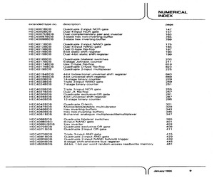
gue multiplexer/demultiplexer 393 HEF4068BD 8-input NAND gate 401 HEF4068BP 8-input NAND gate 401 HEF4068BT 8-input NAND gate 401 HEF406SUBD Hex inverter 403 HEF4069UBP Hex inverter 403 HEF4069UBT Hex inverter 403 HEF4070BD Quadruple exclusive-OR gate 409 HEF4070BP Quadruple exclusive-OR gate 409 HEF4070BT Quadruple. exclusive-OR gate 409 HEF4071BD Quadruple. 2-input OR gate 411 HEF4071BP Quadruple 2-input OR gate 411 HEF4071BT Quadruple 2-input OR gate 411 HEF4072BD Dual 4-input OR gate 413 HEF4072BP Dual 4-input OR gate 413 HEF4072BT Dual 4-input. OR. gate 413 HEF4073BD Triple 3-input AND. gate 415 HEF4073BP Triple 3-input AND gate 415 HEF4073BT Triple 3-input AND gate 415 HEF4075BD Triple 3-input OR gate 417 HEF4075BP Triple 3-input OR gate 417 HEF4075BT Triple 3-input OR gate 417 HEF4076BD Quadruple D-type register with 3-state outputs 419 HEF4076BP Quadruple D-type register with 3-state outputs 419 HEF4076BT Quadruple D-type register with 3-state outputs 419 HEF4077BD Quadruple exclusive-NOR
 11 Pages, 467 KB, Scan
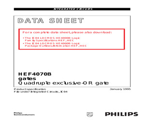
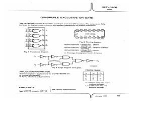
tion HEF4070B gates Quadruple exclusive-OR gate DESCRIPTION The HEF4070B provides the positive quadruple exclusive-OR function. The outputs are fully buffered for highest noise immunity and pattern insensitivity of output impedance. Fig.2 Pinning diagram. HEF4070BP(N): 14-lead DIL; plastic (SOT27-1) HEF4070BD(F): 14-lead DIL; ceramic (cerdip) (SOT73) HEF4070BT(D): 14-lead SO; plastic (SOT108-1) ( ): Package Designator North America Fig.1 Functional diagram. Fig.3 Logic diagram (one gate). TRUTH TABLE APPLICATION INFORMATION Some examples of applications for the HEF4070B are: I1 I2 O1 * Logical comparators L L L * Parity checkers and generators H L H L H H H H L FAMILY DATA, IDD LIMITS category GATES See Family Specifications Note 1. H = HIGH state (the more positive voltage) L = LOW state (the less positive voltage) January 1995 2 Philips Semiconductors Product specification HEF4070B gates Quadruple exclusive-OR gate AC CHARACTERISTICS VSS = 0 V; Tamb = 25 C; CL = 50 pF; input transition times 20
 5 Pages, 47 KB, Original
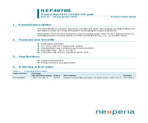
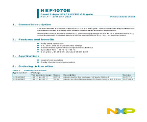
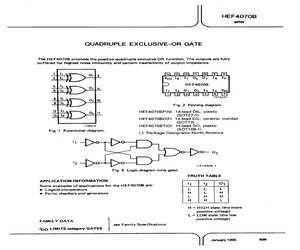
ics Specified from 40 C to +85 C Complies with JEDEC standard JESD 13-B 3. Applications Logical comparators Parity checkers and generators 4. Ordering information Table 1. Ordering information Type number Package Temperature range Name Description Version HEF4070BP 40 C to +85 C DIP14 plastic dual in-line package; 14 leads (300 mil) SOT27-1 HEF4070BT 40 C to +85 C SO14 plastic small outline package; 14 leads; body width 3.9 mm SOT108-1 HEF4070B NXP Semiconductors Quad 2-input EXCLUSIVE-OR gate 5. Functional diagram $ % < $ % < $ % < $ % < A Y B mna788 DDD Fig 1. Functional diagram Fig 2. Logic diagram (one gate) 6. Pinning information 6.1 Pinning HEF4070B 1A 1 14 VDD 1B 2 13 4B 1Y 3 12 4A 2Y 4 11 4Y 2A 5 10 3Y 2B 6 9 3B VSS 7 8 3A aaa-011932 Fig 3. Pin configuration 6.2 Pin description Table 2. Pin description Symbol Pin Description 1A, 2A, 3A, 4A 1, 5, 8, 12 data input 1B, 2B, 3B, 4B 2, 6, 9, 13 data input 1Y, 2Y, 3Y, 4Y 3, 4, 10, 11 data output VSS 7 ground (0 V) VDD 14 supply voltage HEF4070B
 12 Pages, 208 KB, Original
tion HEF4070B gates Quadruple exclusive-OR gate DESCRIPTION The HEF4070B provides the positive quadruple exclusive-OR function. The outputs are fully buffered for highest noise immunity and pattern insensitivity of output impedance. Fig.2 Pinning diagram. HEF4070BP(N): 14-lead DIL; plastic (SOT27-1) HEF4070BD(F): 14-lead DIL; ceramic (cerdip) (SOT73) HEF4070BT(D): 14-lead SO; plastic (SOT108-1) ( ): Package Designator North America Fig.1 Functional diagram. Fig.3 Logic diagram (one gate). TRUTH TABLE APPLICATION INFORMATION Some examples of applications for the HEF4070B are: I1 I2 O1 * Logical comparators L L L * Parity checkers and generators H L H L H H H H L FAMILY DATA, IDD LIMITS category GATES See Family Specifications Note 1. H = HIGH state (the more positive voltage) L = LOW state (the less positive voltage) January 1995 2 Philips Semiconductors Product specification HEF4070B gates Quadruple exclusive-OR gate AC CHARACTERISTICS VSS = 0 V; Tamb = 25 C; CL = 50 pF; input transition times 20
 3 Pages, 28 KB, Original
tion HEF4070B gates Quadruple exclusive-OR gate DESCRIPTION The HEF4070B provides the positive quadruple exclusive-OR function. The outputs are fully buffered for highest noise immunity and pattern insensitivity of output impedance. Fig.2 Pinning diagram. HEF4070BP(N): 14-lead DIL; plastic (SOT27-1) HEF4070BD(F): 14-lead DIL; ceramic (cerdip) (SOT73) HEF4070BT(D): 14-lead SO; plastic (SOT108-1) ( ): Package Designator North America Fig.1 Functional diagram. Fig.3 Logic diagram (one gate). TRUTH TABLE APPLICATION INFORMATION Some examples of applications for the HEF4070B are: I1 I2 O1 * Logical comparators L L L * Parity checkers and generators H L H L H H H H L FAMILY DATA, IDD LIMITS category GATES See Family Specifications Note 1. H = HIGH state (the more positive voltage) L = LOW state (the less positive voltage) January 1995 2 Philips Semiconductors Product specification HEF4070B gates Quadruple exclusive-OR gate AC CHARACTERISTICS VSS = 0 V; Tamb = 25 C; CL = 50 pF; input transition times 20
 4 Pages, 32 KB, Original
52 HEF4071BP,652 HEF4071BT,652 HEF4068BP,652 HEF4023BP,652 HEF4011BP,652 HEF4011BT,652 HEF4011UBP,652 HEF4093BP,652 HEF4093BT,652 HEF4093BT,653 HEF4002BP,652 HEF4002BT,652 HEF4025BP,652 HEF4001BT,652 HEF4001BP,652 HEF4001BT,652 HEF4030BP,652 HEF4030BT,652 HEF4070BP,652 Package 5-TSSOP 5-TSSOP 5-TSSOP 14-TSSOP 14-TSSOP 14-SOIC 20-TSSOP 20-TSSOP 48-TSSOP 8 Price No. of Each No. of Inputs per Circuit Package Stock No. 1-24 Description Circuits AND Gate 2 4 14-DIP 70R5283 0.25 0.48 AND Gate 3 3 14-DIP 70R5271 0.38 0.48 AND Gate 4 2 14-DIP 70R5280 0.38 0.48 AND Gate 4 2 14-SOIC 70R5281 0.29 0.36 70R5268 0.38 0.48 OR Gate 2 4 14-DIP OR Gate 3 3 14-DIP 70R5274 0.25 0.48 OR Gate 4 2 14-DIP 70R5265 0.38 0.48 0.27 OR Gate 4 2 14-SOIC 70R5266 0.21 NAND Gate 1 8 14-DIP 70R5253 0.38 0.48 NAND Gate 3 3 14-DIP 70R5175 0.24 0.46 NAND Gate 4 2 14-DIP 70R5137 0.29 0.36 NAND Gate 4 2 14-SOIC 70R5138 0.23 0.28 NAND Gate, Unbuffered 4 2 14-DIP 70R5140 0.20 0.39 NAND Schmitt Trigger 4 2 14-DIP 70R5286 0.29 0.37 NAND S
 375 Pages, 58008 KB, Original
est noise immunity and pattern insensitivity of output impedance. | 01/3 1a) fi3}_fi2|_ fr} fol_fo] [a 2 Von Ig Iy O4 O3 Ig Is 5 0 _ HEF4070B8 4 6 2 1, Ip 01 02 I3 Iq Ves 1] [2] 130 [4t I tel 12 8 7273473 9 03 | 10 ; ; . Fig. 2 Pinning diagram. 12 Oo, [14 HEF4070BP(N): 14-lead DIL; plastic 13 (SOT27-1) HEF4070BD(F): 14-lead DIL; ceramic (cerdip) (SOT73) 1Z69549 HEF4070BT(D): 14-lead SO; plastic Fig. 1 Functional diagram. (SOT108-1) (}: Package Designator North America 1 Po- TAY O 0, 7274505.1 Fig. 3 Logic diagram (one gate). TRUTH TABLE APPLICATION INFORMATION Some examples of applications for the HEF4070B are: 4 l2 O1 @ Logical comparators L L L @ Parity checkers and generators H L H L H H H H L H = HIGH state (the more positive voltage) L = LOW state (the less FAMILY DATA positive voltage) Ipp LIMITS category GATES see Family Specifications ) (sea 1995 409 HEF4070B gates A.C, CHARACTERISTICS Vgs = 0 V: Tamb = 25 C; Cy = 50 pF; input transition times < 20 ns Vpp typical extrapolation Vv symbol t
 2 Pages, 64 KB, Scan
ry Table 12. Revision history Document ID Release date Data sheet status Change notice Supersedes HEF4070B v.5 20151216 Product data sheet - HEF4070B v.4 Modifications: HEF4070B v.4 Modifications: HEF4070B_CNV v.3 HEF4070B Product data sheet * Type number HEF4070BP (SOT27-1) removed. 20140327 Product data sheet - HEF4070B_CNV v.3 * The format of this data sheet has been redesigned to comply with the new identity guidelines of NXP Semiconductors. * Legal texts have been adapted to the new company name where appropriate. 19950101 Product specification - All information provided in this document is subject to legal disclaimers. Rev. 5 -- 16 December 2015 - (c) Nexperia B.V. 2017. All rights reserved 8 of 11 HEF4070B Nexperia Quad 2-input EXCLUSIVE-OR gate 16. Legal information 16.1 Data sheet status Document status[1][2] Product status[3] Definition Objective [short] data sheet Development This document contains data from the objective specification for product development. Preliminary [short] data
 11 Pages, 751 KB, Original
ully: buffered for highest noise immunity and pattern insensitivity of output impedance. I O43 ral fis] fiz} fri) fro) fs] fe Voo Ie 17 O, O3 Ig Is 3 |) HEF4070B 2 I, Ig 0; 02 1s I, Vss Tt [2] Gay tay tsl Le 2 9293073 03 410 Fig. 2 Pinning diagram. O, [11 HEF4070BP(N): 14-lead DIL; plastic (SOT27-1) HEF4070BD(F): 14-lead DIL; ceramic (cerdip) (SOT73) 7269569 HEF4070BT(D): 14-lead SO; plastic Fig. 1. Functional diagram. (SOT108-1) (): Package Designator North America " >o4Do - > | O 0, 2 >o+>o 72Z274805.1 Fig. 3 Logic diagram (one gate). TRUTH TABLE APPLICATION INFORMATION Some examples of applications for the HEF4070B are: ' l2 04 @ Logical comparators L L L @ Parity checkers and generators H L H L H H H H L H = HIGH state (the more positive voltage) L = LOW state (the less FAMILY DATA positive voltage) see Family Specifications ipp LIMITS category GATES \= 409HEF 4070B gates A.C. CHARACTERISTICS Vss = 0 V; Tamb = 25 OC; CL = 50 pF; input transition times < 20 ns typical extrapolation VoD Vv symb
 2 Pages, 51 KB, Scan


