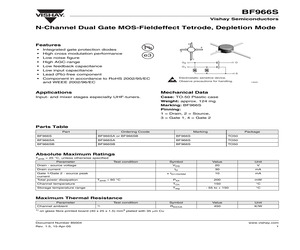
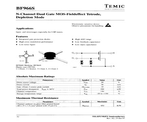
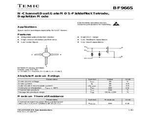
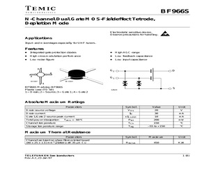
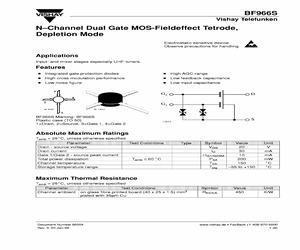
Applications Mechanical Data Input- and mixer stages especially UHF-tuners. Case: TO-50 Plastic case Weight: approx. 124 mg Marking: BF966S Pinning: 1 = Drain, 2 = Source, 3 = Gate 1, 4 = Gate 2 13625 Parts Table Part Ordering Ccode Marking Package BF966S BF966SA or BF966SB BF966S TO50 BF966SA BF966SA BF966S TO50 BF966SB BF966SB BF966S TO50 Absolute Maximum Ratings Tamb = 25 C, unless otherwise specified Parameter Test condition Drain - source voltage Drain current Gate 1/Gate 2 - source peak current Total power dissipation Tamb 60 C Symbol Value Unit VDS 20 V ID 30 mA IG1/G2SM 10 mA mW Ptot 200 Channel temperature TCh 150 C Storage temperature range Tstg - 55 to + 150 C Symbol Value Unit RthChA 450 K/W Maximum Thermal Resistance Parameter Channel ambient 1) Test condition 1) on glass fibre printed board (40 x 25 x 1.5) mm3 plated with 35 m Cu Document Number 85004 Rev. 1.5, 15-Apr-05 www.vishay.com 1 BF966S Vishay Semiconductors Electrical DC Characteristics Tamb = 25 C
 8 Pages, 158 KB, Original
Applications Mechanical Data Input- and mixer stages especially UHF-tuners. Case: TO-50 Plastic case Weight: approx. 124 mg Marking: BF966S Pinning: 1 = Drain, 2 = Source, 3 = Gate 1, 4 = Gate 2 13625 Parts Table Part Ordering Ccode Marking Package BF966S BF966SA or BF966SB BF966S TO50 BF966SA BF966SA BF966S TO50 BF966SB BF966SB BF966S TO50 Absolute Maximum Ratings Tamb = 25 C, unless otherwise specified Parameter Test condition Drain - source voltage Drain current Gate 1/Gate 2 - source peak current Total power dissipation Tamb 60 C Symbol Value Unit VDS 20 V ID 30 mA IG1/G2SM 10 mA mW Ptot 200 Channel temperature TCh 150 C Storage temperature range Tstg - 55 to + 150 C Symbol Value Unit RthChA 450 K/W Maximum Thermal Resistance Parameter Channel ambient 1) Test condition 1) on glass fibre printed board (40 x 25 x 1.5) mm3 plated with 35 m Cu Document Number 85004 Rev. 1.5, 15-Apr-05 www.vishay.com 1 BF966S Vishay Semiconductors Electrical DC Characteristics Tamb = 25 C
 7 Pages, 320 KB, Original
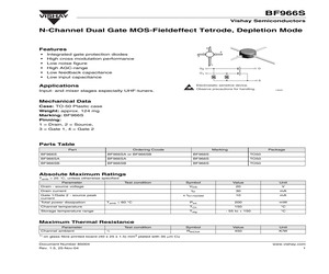
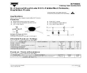
or handling. Input- and mixer stages especially UHF-tuners. 13625 Mechanical Data Case: TO-50 Plastic case Weight: approx. 124 mg Marking: BF966S Pinning: 1 = Drain, 2 = Source, 3 = Gate 1, 4 = Gate 2 Parts Table Part Ordering Ccode Marking Package BF966S BF966SA or BF966SB BF966S TO50 BF966SA BF966SA BF966S TO50 BF966SB BF966SB BF966S TO50 Absolute Maximum Ratings Tamb = 25 C, unless otherwise specified Parameter Test condition Drain - source voltage Drain current Gate 1/Gate 2 - source peak current Tamb 60 C Symbol Value Unit VDS 20 V ID 30 mA IG1/G2SM 10 mA mW Ptot 200 Channel temperature TCh 150 C Storage temperature range Tstg - 55 to + 150 C Symbol Value Unit RthChA 450 K/W Total power dissipation Maximum Thermal Resistance Parameter Channel ambient 1) Test condition 1) on glass fibre printed board (40 x 25 x 1.5) mm3 plated with 35 m Cu Document Number 85004 Rev. 1.5, 25-Nov-04 www.vishay.com 1 BF966S VISHAY Vishay Semiconductors Electrical DC Characteristics Tamb
 8 Pages, 183 KB, Original
S = 0 V(BR)G2SS Typ Max Unit V 8 14 V 8 14 V VG1S = 5 V, VG2S = VDS = 0 IG1SS 50 nA VG2S = 5 V, VG1S = VDS = 0 IG2SS 50 nA -VG1S(OFF) 18 10.5 18 2.5 mA mA mA V -VG2S(OFF) 2.0 V Max Unit mS pF pF fF pF dB dB dB dB dB VDS = 15 V, VG1S = 0, VG2S = 4 V BF966S BF966SA BF966SB IDSS IDSS IDSS 4 4 9.5 Electrical AC Characteristics VDS = 15 V, ID = 10 mA, VG2S = 4 V, f = 1 MHz , Tamb = 25_C, unless otherwise specified Parameter Forward transadmittance Gate 1 input capacitance Gate 2 input capacitance Feedback capacitance Output capacitance Power g gain AGC range Noise figure g Test Conditions VG1S = 0, VG2S = 4 V GS = 2 mS, GL = 0.5 mS, f = 200 MHz GS = 3,3 mS, GL = 1 mS, f = 800 MHz VG2S = 4 to -2 V, f = 800 MHz GS = 2 mS, GL = 0.5 mS, f = 200 MHz GS = 3,3 mS, GL = 1 mS, f = 800 MHz www.vishay.de * FaxBack +1-408-970-5600 2 (8) Symbol y21s Cissg1 Cissg2 Crss Coss Gps Gps DGps F F Min 15 Typ 18.5 2.2 1.1 25 0.8 25 18 40 1.0 1.8 2.6 35 1.2 Document Number 85004 Rev. 3, 20-Jan-99 BF966S Vishay Telefunken Ty
 8 Pages, 93 KB, Original
ig2s = 10 mA, Veis = Vps = 0 +VBr)G2ss 8 14 Vv Gate 1I-source leakage current tVois=5 V. Vo2s = Vps = 0 tIgGiss 50 nA Gate 2-source leakage current +VG25 = 5 V. Vois = Vps = 0 tIgoss 50 nA Drain current BF966S Ipss 4 18 mA Vps = 15 V, Vois = 9, Voas = 4 V BF966SA Ipss 4 10.5 mA BF966SB Ipss 9.5 18 mA Gate 1-source cut-off voltage Vps = 15 V, Va2s =4 V, Ip = 20 uA -VGIS(OFF) 2.5 Vv Gate 2-source cut-off voltage : Vps = 15 V, Vois = 0, Ip = 20 pA i VG2S(OFF) 2.0 Vv Electrical AC Characteristics Vps = 15 V, Ip= 10 mA, Vg2s5 = 4 V, f = | MHz, Tamp = 25C, unless otherwise specified Parameters / Test Conditions | Symbol | Min. | Typ. Unit Forward transadmittance lors | 15 18.5 mS Gate 1-input capacitance Cisse 2.2 2.6 pF Gate 2-input capacitance Vais = 9, Voas = 4 V Cissy? il pF Feedback capacitance Criss 25 35 fF Output capacitance Cass 0.8 1.2 pF Power gain gs = 2 mS, gp = 0.5 mS, f = 200 MHz Gps 25 dB gs = 3.3 mS, g_ = 1 mS, f = 800 MHz Gps 18 dB AGC range Vo2s = 4... -2 V, f = 800 MHz AGps 40 dB No
 7 Pages, 186 KB, Scan
 50 18 10.5 18 nA mA mA mA -VG1S(OFF) 2.5 V -VG2S(OFF) 2.0 V Max. 2.6 Unit mS pF 35 1.2 pF fF pF IG2SS Gate 1-source cut-off voltage VDS = 15 V, VG2S = 4 V, ID = 20 mA Gate 2-source cut-off voltage VDS = 15 V, VG1S = 0, ID = 20 mA IDSS Unit V IG1SS BF966S BF966SA BF966SB Max. 4 4 9.5 Electrical AC Characteristics VDS = 15 V, ID = 10 mA, VG2S = 4 V, f = 1 MHz, Tamb = 25C, unless otherwise specified Parameters / Test Conditions Forward transadmittance Gate 1-input capacitance Gate 2-input capacitance VG1S = 0, VG2S = 4 V Feedback capacitance Output capacitance Power gain VDS = 15 V, ID = 10 mA, VG2S = 4 V, gS = 2 mS, gL = 0.5 mS, f = 200 MHz gS = 3.3 mS, gL = 1 mS, f = 800 MHz AGC range VDS = 15 V, VG2S = 4... -2 V, f = 800 MHz Noise figure VDS = 15 V, ID = 10 mA, VG2S = 4 V, gS = 2 mS, f = 200 MHz f = 800 MHz 2 (6) Symbol y21s Cissg1 Min. 15 Typ. 18.5 2.2 Cissg2 Crss Coss 1.1 25 0.8 Gps Gps 25 18 nGps F F 40 dB dB dB 1.0 1.8 dB dB TELEFUNKEN Semiconductors Rev. A2, 23-Jan-97 BF966S Typical Charact
 6 Pages, 60 KB, Original
S = 0 V(BR)G2SS Typ Max Unit V 8 14 V 8 14 V VG1S = 5 V, VG2S = VDS = 0 IG1SS 50 nA VG2S = 5 V, VG1S = VDS = 0 IG2SS 50 nA -VG1S(OFF) 18 10.5 18 2.5 mA mA mA V -VG2S(OFF) 2.0 V Max Unit mS pF pF fF pF dB dB dB dB dB VDS = 15 V, VG1S = 0, VG2S = 4 V BF966S BF966SA BF966SB IDSS IDSS IDSS 4 4 9.5 Electrical AC Characteristics VDS = 15 V, ID = 10 mA, VG2S = 4 V, f = 1 MHz , Tamb = 25_C, unless otherwise specified Parameter Forward transadmittance Gate 1 input capacitance Gate 2 input capacitance Feedback capacitance Output capacitance Power g gain AGC range Noise figure g www.vishay.com 2 (8) Test Conditions VG1S = 0, VG2S = 4 V GS = 2 mS, GL = 0.5 mS, f = 200 MHz GS = 3,3 mS, GL = 1 mS, f = 800 MHz VG2S = 4 to -2 V, f = 800 MHz GS = 2 mS, GL = 0.5 mS, f = 200 MHz GS = 3,3 mS, GL = 1 mS, f = 800 MHz Symbol y21s Cissg1 Cissg2 Crss Coss Gps Gps DGps F F Min 15 Typ 18.5 2.2 1.1 25 0.8 25 18 40 1.0 1.8 2.6 35 1.2 Document Number 85004 Rev. 3, 20-Jan-99 BF966S Vishay Telefunken Typical Characteristics (Ta
 8 Pages, 96 KB, Original
 = 20 mA Gate 2-source cut-off voltage VDS = 15 V, VG1S = 0, ID = 20 mA Type Symbol Min. Typ. V(BR)DS 20 V(BR)G1SS 8 14 V V(BR)G2SS 8 14 V 50 nA 50 18 10.5 18 nA mA mA mA -VG1S(OFF) 2.5 V -VG2S(OFF) 2.0 V Max. Unit IG2SS IDSS IDSS IDSS Unit V IG1SS BF966S BF966SA BF966SB Max. 4 4 9.5 Electrical AC Characteristics VDS = 15 V, ID = 10 mA, VG2S = 4 V, f = 1 MHz, Tamb = 25C, unless otherwise specified Parameters / Test Conditions Symbol Min. Typ. Forward transadmittance y21s 15 18.5 Gate 1-input capacitance Cissg1 2.2 2.6 pF Gate 2-input capacitance VG1S = 0, VG2S = 4 V Feedback capacitance Cissg2 Crss 1.1 25 35 pF fF Coss 0.8 1.2 pF Gps Gps 25 18 Output capacitance Power gain gS = 2 mS, gL = 0.5 mS, f = 200 MHz gS = 3.3 mS, gL = 1 mS, f = 800 MHz AGC range VG2S = 4... -2 V, f = 800 MHz Noise figure gS = 2 mS, gL = 0.5 mS, f = 200 MHz gS = 3.3 mS, gL = 1 mS, f = 800 MHz 2 (8) nGps F F 40 mS dB dB dB 1.0 1.8 dB dB TELEFUNKEN Semiconductors Rev. A2, 23-Jan-97 BF966S Typical Characteristics (Tj = 25_C u
 8 Pages, 103 KB, Original
S = 0 V(BR)G2SS Typ Max Unit V 8 14 V 8 14 V VG1S = 5 V, VG2S = VDS = 0 IG1SS 50 nA VG2S = 5 V, VG1S = VDS = 0 IG2SS 50 nA -VG1S(OFF) 18 10.5 18 2.5 mA mA mA V -VG2S(OFF) 2.0 V Max Unit mS pF pF fF pF dB dB dB dB dB VDS = 15 V, VG1S = 0, VG2S = 4 V BF966S BF966SA BF966SB IDSS IDSS IDSS 4 4 9.5 Electrical AC Characteristics VDS = 15 V, ID = 10 mA, VG2S = 4 V, f = 1 MHz , Tamb = 25_C, unless otherwise specified Parameter Forward transadmittance Gate 1 input capacitance Gate 2 input capacitance Feedback capacitance Output capacitance Power g gain AGC range Noise figure g www.vishay.com 2 (8) Test Conditions VG1S = 0, VG2S = 4 V GS = 2 mS, GL = 0.5 mS, f = 200 MHz GS = 3,3 mS, GL = 1 mS, f = 800 MHz VG2S = 4 to -2 V, f = 800 MHz GS = 2 mS, GL = 0.5 mS, f = 200 MHz GS = 3,3 mS, GL = 1 mS, f = 800 MHz Symbol y21s Cissg1 Cissg2 Crss Coss Gps Gps DGps F F Min 15 Typ 18.5 2.2 1.1 25 0.8 25 18 40 1.0 1.8 2.6 35 1.2 Document Number 85004 Rev. 3, 20-Jan-99 BF966S Vishay Semiconductors Typical Characteristics
 8 Pages, 149 KB, Original
eis = Vps = 0 +V(BR)G2SS 8 14 Vv breakdown voltage Gate 1 - source tVeis=5V, Veos = Vps = 0 tleiss 50 nA leakage current Gate 2 - source tVees =5 V, Veis = Vps = 0 tleass 50 nA leakage current Drain current Vos =15V, Veis = 0, Vees =4V BF966S loss 4 18 mA BF966SA | __Inss 4 10.5 | mA BF966SB loss 9.5 18 mA Gate 1 - source Vos =15V, Vees =4V, Ip = 20 VG1S(OFF) 25 Vv cut-off voltage vA Gate 2 - source Vos =15V, Veis = 0, ID =20 vA VG2s(OFF) 2.0 Vv cut-off voltage Electrical AC Characteristics Vos = 15 V, Ip = 10 MA, Veos = 4 V, f= 1 MHZ, Tamp = 25C, unless otherwise specified Forward transadmittance | Y21s | 15 | 18.5 ms Gate 1 input capacitance Cissai 2.2 | 26 | pF Gate 2 input capacitance |Veig =0, Veg = 4V Cissq2 1.1 pF Feedback capacitance Criss 25 35 | fF Output capacitance Coss 0.8 | 1.2 | pF Power gain Gg =2 mS, G, = 0.5 mS, f = 200 MHz Gog 25 dB Gg = 3,3 mS, G, = 1 mS, f = 800 MHz Gog 18 dB AGC range Ves = 4 to -2 V, f = 800 MHz AGops 40 dB Noise figure Gg =2 mS, G, = 0.5 mS, f = 200 MHz F
 8 Pages, 254 KB, Scan


