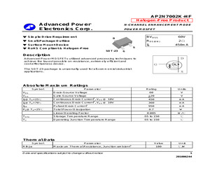
2N7002K-HF Halogen-Free Product Advanced Power Electronics Corp. N-CHANNEL ENHANCEMENT MODE POWER MOSFET Simple Drive Requirement D Small Package Outline Surface Mount Device BVDSS 60V RDS(ON) 2 ID 450mA S RoHS Compliant & Halogen-Free SOT-23 G Description D Advanced Power MOSFETs utilized advanced processing techniques to achieve the lowest possible on-resistance, extremely efficient and cost-effectiveness device. G The SOT-23 package is universally used for all commercial-industrial applications. S Absolute Maximum Ratings Parameter Symbol VDS Drain-Source Voltage VGS Gate-Source Voltage ID@TA=25 ID@TA=70 Rating Units 60 V +20 V 3 450 mA 3 360 mA Continuous Drain Current , VGS @ 10V Continuous Drain Current , VGS @ 10V 1 IDM Pulsed Drain Current 950 mA PD@TA=25 Total Power Dissipation 0.7 W Linear Derating Factor 0.005 W/ TSTG Storage Temperature Range -55 to 150 TJ Operating Junction Temperature Range -55 to 150 Thermal Data Symbol Rthj-a Parameter Maximum Thermal Resistance, Junction-ambient
 4 Pages, 59 KB, Original
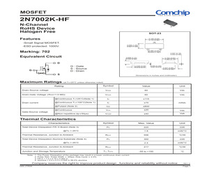
2N7002K-HF N-Channel RoHS Device Halogen Free SOT-23 Features 0.120 (3.04) 0.110 (2.80) -Small Signal MOSFET. 3 0.055 (1.40) 0.047 (1.20) -ESD protected: 1000V. 2 1 0.080 (2.04) 0.070 (1.78) Marking: 702 Equivalent Circuit 0.044 (1.11) 0.035 (0.89) 0.007 (0.18) 0.003 (0.08) 0.104 (2.64) 0.083 (2.10) D G : Gate S : Source D : Drain G 0.020 (0.50) 0.015 (0.37) S 0.004 (0.100) 0.001 (0.013) 0.027 (0.69) 0.014 (0.35) Dimensions in inches and (millimeter) Maximum Ratings (at T =25C unless otherwise noted) A Symbol Value Unit Drain-Source voltage VDSS 60 Vdc Drain-Gate Voltage (RGS=1.0 M) VDGR 60 Vdc @Continuous TC=25C(Note 1) ID 115 @Continuous TC=100C(Note 1) ID 75 @Pulsed (Note 2) IDM 800 @Continuous VGS 20 Vdc VGSM 40 Vpk Symbol Max. Value Unit PD 225 mW 1.8 mW/C RJA 556 C/W PD 300 mW 2.4 mW/C RJA 417 C/W TJ, TSTG -55 to +150 C Rating Drain current mAdc Gate-Source voltage @Non-repetitive (tp50s) Thermal Characteristics Characteristics Total Device Dissipation FR-5 Board (Note 3) @TA = 25C Thermal
 5 Pages, 118 KB, Original


