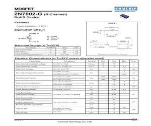
2N7002-G (N-Channel) RoHS Device Features SOT-23 Power dissipation : 0.35W 0.119(3.00) 0.110(2.80) Equivalent Circuit D 0.056(1.40) 0.047(1.20) D G G 0.006(0.15) 0.002(0.05) 0.044(1.10) 0.035(0.90) S Maximum Ratings (at T =25C) A Parameter Drain-Source voltage 0.103(2.60) 0.086(2.20) 0.020(0.50) 0.013(0.35) Symbol Value Unit VDS 60 V Drain current ID 250 mA Power dissipation PD 350 mW TJ, TSTG -55 ~ +150 C Junction and storage temperature S 0.083(2.10) 0.066(1.70) G : Gate S : Source D : Drain 0.006(0.15)max 0.007(0.20)min Dimensions in inches and (millimeter) Electrical Characteristics (at TA=25C unless otherwise noted) Parameter Conditions Drain-Source breakdown voltage VGS=0V, ID=10A Gate-Threshold voltage VDS=VGS, ID=250A Gate-body leakage VDS=0V, VGS=15V Symbol Min Typ V(BR)DSS 60 70 Vth(GS) 1 1.5 Max Unit V IGSS 10 VDS=60V, VGS=0V Zero gate voltage drain current 2.5 1 IDSS A 500 VDS=60V, VGS=0V, TJ=125C VGS=10V, VDS=7.5V On-state drain current 800 1300 500 700 ID(ON) VGS=4.5V, VDS=10V VGS=1
 5 Pages, 108 KB, Original
2N7002-G (N-Channel) RoHS Device Features SOT-23 Power dissipation : 0.35W 0.119(3.00) 0.110(2.80) Equivalent Circuit D 0.056(1.40) 0.047(1.20) D G G 0.006(0.15) 0.002(0.05) 0.044(1.10) 0.035(0.90) S 0.103(2.60) 0.086(2.20) Maximum Ratings (at TA=25C) Parameter S 0.083(2.10) 0.066(1.70) G : Gate S : Source D : Drain Symbol Value Unit VDS 60 V 0.020(0.50) 0.013(0.35) 0.006(0.15)max 0.007(0.20)min Drain-Source voltage Drain current ID 250 mA Power dissipation PD 350 mW TJ, TSTG -55 ~ +150 C Junction and storage temperature Dimensions in inches and (millimeter) Electrical Characteristics (at TA=25C unless otherwise noted) Parameter Conditions Drain-Source breakdown voltage VGS=0V, ID=10A Gate-Threshold voltage VDS=VGS, ID=250A Gate-body leakage VDS=0V, VGS=15V Symbol Min Typ V(BR)DSS 60 70 Vth(GS) 1 1.5 Max Unit V IGSS 10 VDS=60V, VGS=0V Zero gate voltage drain current 2.5 1 IDSS A 500 VDS=60V, VGS=0V, TJ=125C VGS=10V, VDS=7.5V On-state drain current 800 1300 500 700 ID(ON) VGS=4.5V, VDS=10V VGS=10V
 4 Pages, 173 KB, Original
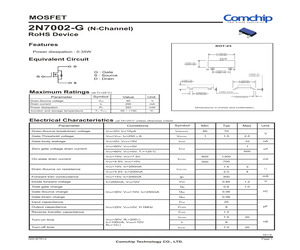
2N7002-G (N-Channel) RoHS Device Features SOT-23 Power dissipation : 0.35W 0.119(3.00) 0.110(2.80) Equivalent Circuit D 0.056(1.40) 0.047(1.20) D G G 0.006(0.15) 0.002(0.05) 0.044(1.10) 0.035(0.90) S Maximum Ratings (at T =25C) A Parameter Drain-Source voltage 0.103(2.60) 0.086(2.20) 0.020(0.50) 0.013(0.35) Symbol Value Unit VDS 60 V Drain current ID 250 mA Power dissipation PD 350 mW TJ, TSTG -55 ~ +150 C Junction and storage temperature S 0.083(2.10) 0.066(1.70) G : Gate S : Source D : Drain 0.006(0.15)max 0.007(0.20)min Dimensions in inches and (millimeter) Electrical Characteristics (at TA=25C unless otherwise noted) Parameter Conditions Drain-Source breakdown voltage VGS=0V, ID=10A Gate-Threshold voltage VDS=VGS, ID=250A Gate-body leakage VDS=0V, VGS=15V Symbol Min Typ V(BR)DSS 60 70 Vth(GS) 1 1.5 Max Unit V IGSS 10 VDS=60V, VGS=0V Zero gate voltage drain current 2.5 1 IDSS A 500 VDS=60V, VGS=0V, TJ=125C VGS=10V, VDS=7.5V On-state drain current 800 1300 500 700 ID(ON) VGS=4.5V, VDS=10V VGS=1
 4 Pages, 107 KB, Original
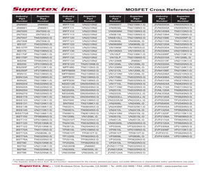
 689-TN0604N3-G 689-TN2504N8-G 689-TN0104N3-G 689-TN0104N8-G 689-VN0104N3-G 689-VN3205N3-G 689-VN3205N8-G 689-TN0606N3-G 689-TN2106K1-G 689-TN2106N3-G 689-TN0106N3-G 689-VN2222LL-G 689-VN0606L-G 689-VN0106N3-G 689-VN2106N3-G 689-VN10KN3-G 689-2N7000-G 689-2N7002-G 689-VN0808L-G 689-TN0610N3-G 689-TN2510N8-G 689-TN0110N3-G 689-VN2210N3-G 689-VN2110K1-G 689-VN1206L-G 689-TN0620N3-G 689-TD9944TG-G 689-TN2524N8-G 689-VN2406L-G (c) Copyright 2016 Mouser Electronics 748 Supertex Part No. TN2501N8-G TN0702N3-G VN0300L-G TN0604N3-G TN2504N8-G TN0104N3-G TN0104N8-G VN0104N3-G VN3205N3-G VN3205N8-G TN0606N3-G TN2106K1-G TN2106N3-G TN0106N3-G VN2222LL-G VN0606L-G VN0106N3-G VN2106N3-G VN10KN3-G 2N7000-G 2N7002-G VN0808L-G TN0610N3-G TN2510N8-G TN0110N3-G VN2210N3-G VN2110K1-G VN1206L-G TN0620N3-G TD9944TG-G TN2524N8-G VN2406L-G Package Type SOT-89-3 TO-92 TO-92 TO-92 SOT-89-3 TO-92 SOT-89-3 TO-92 TO-92 SOT-89-3 TO-92 SOT-23-3 TO-92 TO-92 TO-92 TO-92 TO-92 TO-92 TO-92 TO-92 SOT-23-3 TO-92 TO-92
 1 Pages, 256 KB, Original
N3-GTO-92 Yes 689-TN0106N3-G TN0106N3-GTO-92 Yes 689-VN2222LL-G VN2222LL-GTO-92 Yes 689-VN0606L-G VN0606L-GTO-92 Yes 689-VN0106N3-G VN0106N3-GTO-92 Yes 689-VN2106N3-G VN2106N3-GTO-92 Yes 689-VN10KN3-G VN10KN3-GTO-92 Yes 689-2N7000-G 2N7000-G TO-92 Yes 689-2N7002-G 2N7002-GSOT-23-3Yes 689-VN0808L-G VN0808L-GTO-92 Yes 689-TN0610N3-G TN0610N3-GTO-92 Yes 689-TN2510N8-G TN2510N8-GSOT-89-3 Yes 689-TN0110N3-G TN0110N3-GTO-92 Yes 689-VN2210N3-G VN2210N3-GTO-92 Yes 689-VN2110K1-G VN2110K1-GSOT-23-3 Yes 689-VN1206L-G VN1206L-GTO-92 Yes 689-TN0620N3-G TN0620N3-GTO-92 Yes Yes 689-TD9944TG-G TD9944TG-G SOIC-8 689-TN2524N8-G TN2524N8-GSOT-89-3 Yes 689-VN2406L-G VN2406L-GTO-92 Yes (c) Copyright 2011 Mouser Electronics 500 mouser.com/supertex 18 20 30 40 40 40 40 40 50 50 60 60 60 60 60 60 60 60 60 60 60 80 100 100 100 100 100 120 200 240 240 240 0.3 1 0.5 1 0.8 2.5 0.6 1.6 0.6 1.6 0.6 1.6 0.6 1.6 0.8 2.4 0.8 2.4 0.8 2.4 0.6 2 0.6 2 0.6 2 0.6 2 0.6 2.5 0.8 2 0.8 2.4 0.8 2.4 0.8 2.5 0.83.0 1 2.5 0.8
 379 Pages, 47721 KB, Original
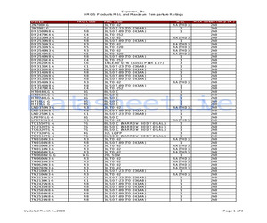
try Part Number Supertex Part Number 2N6660 2N6660 IRFF110 VN2210N2 VN0605T TN2106K1-G ZVN0540A VN0550N3-G 2N6661 2N6661 IRFF111 VN2210N2 VN0606L TN2106N3-G ZVN0545A VN0550N3-G 2N7000 2N7000-G IRFF112 VN2210N2 VN0606M TN2106N3-G ZVN1409A TN0110N3-G 2N7002 2N7002-G IRFF113 VN2210N2 VN0610L TN2106N3-G ZVN2106A TN2106N3-G 2N7007 TN5325N3-G IRFF120 VN2210N2 VN0610LL TN2106N3-G ZVN2106E VN3205P-G 2N7008 2N7008-G IRFF121 VN2210N2 VN0808L VN0808L-G ZVN2110A TN0110N3-G BS107 TN5325N3-G IRFF122 VN2210N2 VN0808M VN0808L-G ZVN2120A TN5325N3-G BS107P TN5325N3-G IRFF123 VN2210N2 VN10KM VN10KN3-G ZVN2535A TN2540N3-G BS170 TN2106N3-G IRFF130 VN2210N2 VN10KN3 VN10KN3-G ZVN3306A VN2106N3-G BS170F TN2106K1-G IRFF131 VN2210N2 VN10LF TN2106K1-G ZVN3306F VN2110K1-G BS170P TN2106N3-G IRFF132 VN2210N2 VN10LP TN2106N3-G ZVN3310A VN1206L-G BS208 TP0620N3-G IRFF133 VN2210N2 VN1206B 2N6661 ZVN3310F VN2110K1-G BS250 VP2106N3-G IRFS123 TN2510N8-G VN1206L VN1206L-G ZVN3320A TN5325N3-G BS250F VP2110K1-G MPF480 TN0110N3-G VN120
 1 Pages, 74 KB, Original
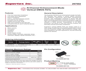
ontrols Converters Amplifiers Switches Power supply circuits Drivers (relays, hammers, solenoids, lamps, memories, displays, bipolar transistors, etc.) Ordering Information RDS(ON) ID(ON) (V) (max) () (min) (A) 60 7.5 0.5 Device Package Option BVDSS/BVDGS 2N7002-G TO-236AB (SOT-23) -G indicates package is RoHS compliant (`Green') Absolute Maximum Ratings Pin Configuration Parameter Value Drain-to-source voltage BVDSS Drain-to-gate voltage BVDGS Gate-to-source voltage 30V Operating and storage temperature Soldering temperature* SOURCE -55C to +150C GATE TO-236AB (SOT-23) +300C Absolute Maximum Ratings are those values beyond which damage to the device may occur. Functional operation under these conditions is not implied. Continuous operation of the device at the absolute rating level may affect device reliability. All voltages are referenced to device ground. * Distance of 1.6mm from case for 10 seconds. DRAIN Product Marking 702W W = Code for week sealed = "Green" Packaging TO-236AB (SOT-23) 2N70
 5 Pages, 577 KB, Original
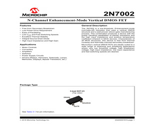
ntal X Media Type Device: 2N7002 = N-Channel Enhancement-Mode Vertical DMOS FET Package: (blank) = 3-lead SOT-23 Environmental: G = Lead (Pb)-free/RoHS-compliant Package Media Type: (blank) = 3000/Reel for an SOT-23 Package DS20005797A-page 12 Example: a) 2N7002-G: N-Channel Enhancement-Mode Vertical DMOS FET, 3-lead SOT-23, 3000/Reel 2018 Microchip Technology Inc. Note the following details of the code protection feature on Microchip devices: * Microchip products meet the specification contained in their particular Microchip Data Sheet. * Microchip believes that its family of products is one of the most secure families of its kind on the market today, when used in the intended manner and under normal conditions. * There are dishonest and possibly illegal methods used to breach the code protection feature. All of these methods, to our knowledge, require using the Microchip products in a manner outside the operating specifications contained in Microchip's Data Sheets. Most likely, the person doing
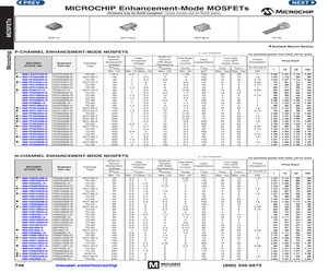
 14 Pages, 884 KB, Original
low input capacitance, and fast switching speeds are desired. Motor controls Converters Amplifiers Switches Power supply circuits Drivers (relays, hammers, solenoids, lamps, memories, displays, bipolar transistors, etc.) Ordering Information Device 2N7002 2N7002-G BVDSS/BVDGS (V) Package TO-236AB (same as SOT-23) RDS(ON) ID(ON) (max) (min) () (A) 7.5 0.5 60 -G indicates package is RoHS compliant (`Green') Pin Configuration DRAIN Absolute Maximum Ratings Parameter Value DRAIN to SOURCE voltage BVDSS DRAIN to GATE voltage BVDGS GATE to SOURCE voltage 30V Operating and storage temperature Soldering temperature1 SOURCE TO-236AB (Top View) -55C to +150C +300C Absolute Maximum Ratings are those values beyond which damage to the device may occur. Functional operation under these conditions is not implied. Continuous operation of the device at the absolute rating level may affect device reliability. All voltages are referenced to device ground. Notes: 1. Distance of 1.6mm from case for 10 seconds. GATE P
 5 Pages, 544 KB, Original
 are desired. Motor controls Converters Amplifiers Switches Power supply circuits Drivers (relays, hammers, solenoids, lamps, memories, displays, bipolar transistors, etc.) Ordering Information Device Package Option BVDSS/BVDGS RDS(ON) ID(ON) (V) (max) () 2N7002-G TO-236AB (SOT-23) 60 7.5 0.5 (min) (A) -G indicates package is RoHS compliant (`Green') Absolute Maximum Ratings Pin Configuration Parameter Value Drain-to-source voltage BVDSS Drain-to-gate voltage BVDGS Gate-to-source voltage 30V Operating and storage temperature Soldering temperature* SOURCE -55C to +150C GATE TO-236AB (SOT-23) +300C Absolute Maximum Ratings are those values beyond which damage to the device may occur. Functional operation under these conditions is not implied. Continuous operation of the device at the absolute rating level may affect device reliability. All voltages are referenced to device ground. * Distance of 1.6mm from case for 10 seconds. DRAIN Product Marking 702W W = Code for week sealed = "Green" Packaging T
 5 Pages, 467 KB, Original
2N7002-G DN1509N8-G DN2470K4-G DN2530N3-G DN2530N8-G DN2535N3-G DN2535N5-G DN2540N3-G DN2540N5-G DN2540N8-G DN2625K4-G DN2625K6-G DN3135K1-G DN3135N8-G DN3145N8-G DN3525N8-G DN3535N8-G DN3545N3-G DN3545N8-G GN2470K4-G HT0440LG-G HT0638LG-G HT0740LG-G HT18LG-G HT19LG-G LND150N3-G LND150N8-G LND250K1-G LP0701LG-G LP0701N3-G TC1550TG-G TC2320TG-G TC6320TG-G TC7320FG-G TD9944TG-G TN0104N3-G TN0104N8-G TN0106N3-G TN0110N3-G TN0604N3-G TN0604WG-G TN0606N3-G TN0610N3-G TN0620N3-G TN0702N3-G TN2106K1-G TN2106N3-G TN2124K1-G TN2130K1-G TN2425N8-G TN2435N8-G TN2501N8-G TN2504N8-G TN2510N8-G TN2524N8-G Updated March 5, 2008 PKG Code N8 K4 N3 N8 N3 N5 N3 N5 N8 K4 K6 K1 N8 N8 N8 N8 N3 N8 K4 LG LG LG LG LG N3 N8 K1 LG N3 TG TG TG FG TG N3 N8 N3 N3 N3 WG N3 N3 N3 N3 K1 N3 K1 K1 N8 N8 N8 N8 N8 N8 PKG Type 3L TO-92 3L SOT-23 (TO-236AB) 3L SOT-89 (TO-243AA) 3L TO-252 3L TO-92 3L SOT-89 (TO-243AA) 3L TO-92 3L TO-220 3L TO-92 3L TO-220 3L SOT-89 (TO-243AA) 3L TO-252 14 LEAD QFN ( 5x5x1 Pitch 1.27) 3L SOT-23 (TO-236A
 3 Pages, 9 KB, Original


