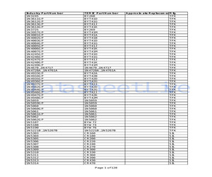
2N5546 2N5547 2N5549 2N5555 2N5556 2N5561 2N5562 2N5563 2N5564 2N5565 2N5566 TEMIC Part Number 2N4340 2N4340 2N4341 2N4341 2N5432 2N5433 2N5434 2N5114 2N5116 2N5196 2N5196 2N5197 2N4416 2N4416 J210 J211 J212 2N4339 2N4341 2N4341 2N4341 2N4341 J212 2N5196 2N5198 2N5199 2N4340 J202 J202 J202 J304 2N5196 2N5197 2N5198 2N5199 2N5199 2N5196 2N5197 2N5198 2N5199 2N5199 2N5197 2N5197 2N5197 2N5198 2N5199 2N4392 2N5486 2N4339 U401 U401 U404 2N5564 2N5565 2N5566 Page 4 of 128 Approximate ReplacemenMfg SIL SIL SIL SIL SIL SIL SIL SIL SIL SIL SIL SIL SIL SIL SIL SIL SIL SIL SIL SIL SIL SIL SIL SIL SIL SIL SIL SIL SIL SIL SIL SIL SIL SIL SIL SIL SIL SIL SIL SIL SIL SIL SIL SIL SIL SIL SIL SIL SIL SIL SIL SIL SIL SIL SIL Industry Part Number 2N5592 2N5593 2N5594 2N5638 2N5639 2N5640 2N5647 2N5648 2N5649 2N5653 2N5654 2N5668 2N5669 2N5670 2N5717 2N5718 2N5801 2N5902 2N5903 2N5904 2N5905 2N5906 2N5907 2N5908 2N5909 2N5949 2N5950 2N5951 2N5952 2N5953 2N6451 2N6452 2N6453 2
 128 Pages, 241 KB, Original
JFET 2N5523 3-37 5-27 2N5158 N JFET 2N5434 2N5524 DN JFET 2N5524 3-37 5-27 2N5159 N JFET 2N5433 2N5545 DN JFET 2N5545 3-38 5-15 2N5196 DN JFET 2N5196 3-34 5-15 2N5546 DN JFET 2N5546 3-38 5-15 2N5197 DN JFET 2N5197 3-34 5-15 2N5547 DN JFET 2N5547 3-38 5-15 2N5198 DN JFET 2N5198 3-34 -15 2N5549 N JFET 2N4392 2N5199 DN JFET 2N5199 3-34 5-15 2N5555 N JFET 2N5555 4-4 5-8 2N5245 N JFET KK4418 2N5556 N JFET 2N5556 3-39 5-25 2N5246 N JFET J305-18 2N5557 N JFET 2N5557 3-39 5-25 2N5247 N UFE 5304-18 2N5558 N JFET 2N5558 3-39 5-25 2N5248 N JFET 2N5486 2N5561 DN JFET 401 2N5257 N JFET 2N5457 2N5562 DN JFET U402 2N5258 N JFET 2N5458 2N5563 DN JFET U404 2N5259 N JFET 2N5459 2N5564 DN JFET 2N5564 3-40 5-3 2N5265 P JFET 2N2608 2N5565 DN JFET 2N5565 3-40 5-3 2N5266 P JFET 2N2608 2N5566 ON JFET 2N5566 3-40 5-3 2N5267 P JFET 2N2608 2N5592 N JFET 2N3822 2N5268 P JFET 2N2608 2N5593 N JFET 2N3822 2N5269 P JFET 2N3331 2N5594 N JFET 2N3822 2N5270 P JFET 2N3331 2N5638 N JFET 2N5638 4-5 5-3 2N5358 N JPET 2N36
 268 Pages, 11688 KB, Scan
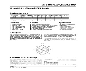
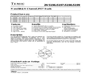
2N5198 0.7 to 4 -50 1 ~15 10 2N5199 0.7 to 4 50 1 ~15 15 Features Benefits Applications Monolithic Design Tight Differential Match vs. Current @ Wideband Differential Amps @ High Slew Rate @ Improved Op Amp Speed, Settling Time Accuracy @ High-Speed, Low Offset/Drift Voltage @ Minimum Input Error/Trimming Requirement Temp-Compensated, Low Gate Leakage: 5 pA Insignificant Signal Loss/Error Voltage Single-Ended Input Amps Low Noise High System Sensitivity High Speed Comparators @ High CMRR: 100 dB Minimum Error with Large Input Signal Impedance Converters Description The 2N5196/5197/S198/5199 JFET duals are designed for high-performance differential amplification for a wide range of precision test instrumentation applications. This series features tightly matched specs, low gate leakage for accuracy, and wide dynamic range with Ig guaranteed at Vpg = 20 V. The hermetically-sealed TO-71 package is available with full military processing (see Military Information and the 2N5545/5546/S547JANTX/JANTXYV
 6 Pages, 219 KB, Scan
2N5198 -0.7 to -4 2N5199 -0.7 to -4 Features Benefits Applications Wideband Differential Amps High-Speed, Temp-Compensated, Single-Ended Input Amps High Speed Comparators Impedance Converters Monolithic Design High Slew Rate Low Offset/Drift Voltage Low Gate Leakage: 5 pA Low Noise High CMRR: 100 dB Tight Differential Match vs. Current Improved Op Amp Speed, Settling Time Accuracy Minimum Input Error/Trimming Requirement Insignificant Signal Loss/Error Voltage High System Sensitivity Minimum Error with Large Input Signal Description The 2N5196/5197/5198/5199 JFET duals are designed for high-performance differential amplification for a wide range of precision test instrumentation applications. This series features tightly matched specs, low gate leakage for accuracy, and wide dynamic range with IG guaranteed at VDG = 20 V. The hermetically-sealed TO-71 package is available with full military processing (see Military Information and the 2N5545/5546/5547JANTX/JANTXV data sheet). For similar products
 6 Pages, 63 KB, Original
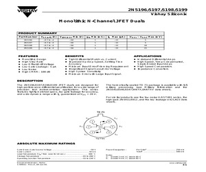
2N5198 -0.7 to -4 -50 1 -15 10 2N5199 -0.7 to -4 -50 1 -15 15 FEATURES BENEFITS APPLICATIONS D D D D D D D Tight Differential Match vs. Current D Improved Op Amp Speed, Settling Time Accuracy D Minimum Input Error/Trimming Requirement D Insignificant Signal Loss/Error Voltage D High System Sensitivity D Minimum Error with Large Input Signal D Wideband Differential Amps D High-Speed, Temp-Compensated, Single-Ended Input Amps D High Speed Comparators D Impedance Converters Monolithic Design High Slew Rate Low Offset/Drift Voltage Low Gate Leakage: 5 pA Low Noise High CMRR: 100 dB DESCRIPTION The 2N5196/5197/5198/5199 JFET duals are designed for high-performance differential amplification for a wide range of precision test instrumentation applications. This series features tightly matched specs, low gate leakage for accuracy, and wide dynamic range with IG guaranteed at VDG = 20 V. The hermetically-sealed TO-71 package is available with full military processing (see Military Information and the 2N55
 7 Pages, 87 KB, Original
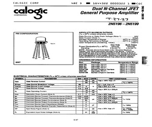
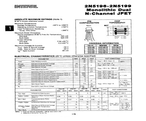
ifications is not implied. Exposure to absolute maximum rating conditions for extended periods may affect device reliability, ORDERING INFORMATION 6037 Part Package Temperature Range 2N5196 ~ Hermetic TO-71 -88C to +150C 2N5197 Hermetic TO-71 55C to +150C 2N5198 Hermetic TO-71 -55C to +150C X2N5198 Sorted Chips in Carriers 55C to +150C 2N5199 ~ Hermetic TO-71 -55C to +150C X2N5199 Sorted Chips in Carriers -55C to +150C ELECTRICAL CHARACTERISTICS (Ta = 25C unless otherwise specified) SYMBOL PARAMETER MIN | MAX | UNITS TEST CONDITIONS -26 pA | Vas =-30V, Vos = 0 I Gate Re Ci t 88 verse warren 50 | nA [Ta = 150C BVass Gate-Source Breakdown Voltage -50 la =-1pA, Vos = 0 Vasiom Gate-Source Cutoff Voltage 0.7 | 4 Vs Voa = 20V, Ip = 1nA Ves Gate-Source Voltage 0.2 = A Voa = 20V, Ip = 200pA la Gate Operating Current 5 7A [Tan 1258 = 108 loss Saturation Drain Current (Note 2) 0.7 7 mA_ | Vos = 20V, Vas #0 Ota Common-Source Forward Transconductance (Note 2) 1000 | 4000 Vos = 20V, Vag = 0 Ots C
 2 Pages, 109 KB, Scan
 One Side 2.56 mwW/C Sr Both Sides 4.3 mw/C ORDERING INFORMATION Maximum Voltages & Currents TO-71 WAFER DICE Vag Gate to Source Voltage ~b0 V 2N5196 | 2N5196/W_| 2N5196/D Vgp Gate to Drain Voltage ~5O0 V 2N5197 | 2N5197/W_| 2N5197/D 1g Gate Current 50 mA 2N5198 | 2N5198/W_| 2N5198/D 2N5199 | 2N5199/W | 2N5199/D 2N5196-2N5199 Monolithic Dual N-Channel JFET 2 op. | =r} ELECTRICAL CHARACTERISTICS (25C unless otherwise specified) PARAMETER MIN MAX UNIT TEST CONDITIONS ! Gate Reverse Current ~% pa Vv 30V,V 0 rr ze ' = = a GSS Reverse Gu 50 | nA Gs DS 160C BVGss Gate-Source Breakdown Voltage -50 ig =-1 uA, Vps=0 VGSioft) Gate-Source Cutoff Voltage -07 4 Vv Vps = 20V, Ip =i nA _ Vos Gate-Source Voltage 0.2 -3.8 . ~15 A Vog = 20 V, Ip = 200 ZA Ig Gate Operating Current 715 mA DG Dd [ C J | loss Saturation Drain Current (Note 1) 0.7 7 mA Vos = 20 V, Ves = 0 Sfs Common-Source Forward Transconductance (Note 1) 1000 4000 Vps = 20 V, VGs =0 fs * Common-Source Forward Transconductanc
 1 Pages, 53 KB, Scan
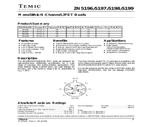
2N5198 2N5199 Applications Wideband Differential Amps High-Speed, Temp-Compensated, Single-Ended Input Amps @ High Speed Comparators Impedance Converters Features Benefits Monolithic Design Tight Differential Match vs. Current High Slew Rate @ Improved Op Amp Speed, Settling Time Accuracy @ Low Offset/Drift Voltage Minimum Input Error/Irimming Requirement @ Low Gate Leakage: 5 pA Insignificant Signal Loss/Error Voltage @ Low Noise High System Sensitivity @ High CMRR: 100 dB @ Minimum Error with Large Input Signal Description The 2N5196/5197/5198/5199 JFET duals are designed for high-performance differential amplification for a wide range of precision test instrumentation applications. This series features tightly matched specs, low gate leakage for accuracy, and wide dynamic range with Ig guaranteed at Vpg = 20 V. The hermetically-sealed TO-71 package is available with full military processing (see Military Information and the 2N5545/5546/SS47JANTX/JANTXV data sheet). For similar products see the
 6 Pages, 227 KB, Scan
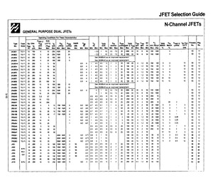
 45 | 05 8/15 6 25 250 30 8 4 50 } 200 10 20 3 83 12 2N5196 TO-71[ 20 200 5 5 15 [| 700 1500 4 02 38107 45 | 07 7 1 4 50 25 30 $ 2 50 20 1000 3 1 5 8&3 12 2N5197 TO-71; 20 200 10 15 | 700 1500 4 0.2 38107 45 | 07 7 1 4 50 2 30 6 2 50 20 1000 5 3 1 5 83 12 2N5198 TO-71} 20 200 0 20 15) 700 1500 4 02 38 )07 45 | 07 7 1 4 50 25 30 6 2 50 20 1000 5 1 5 83 12 2N5199 TO-717 20 200 15 40 17 | 700 1500 4 02 38107 45 | 07 7 1 4 50 25 30 6 2 50 20 1000 5 1 5 83 12 2N5452 TO-71} 20 200 5 5 1 02 42 1 45 105 5 1 3 3 100 30 4 12 50 20 1000 5 3 0.25 83 12 2N5453 TO-71; 20 200 10 10 1 02 42 1 45 105 5 1 3 3 100-30 4 $12 20 1000 5 3 0.25 83 42 2N5454 TO-71}; 20 200 15 25 1 02 42 1 45} 05 1 3 3 100 30 4 12 50 20 1000 5 5 025 83 12 2N5545 TO-71] 15 200 5 10 50 05 45 |] 05 8) 15 6 25 100 30 6 2 50 | 180 10 3 1 5 83 12 2N5546 TO-71} 15 200 10 20 50 05 45 | 05 8445 6 25 100 30 6 2 50 | 200 10 10 5 2 5 83 12 2N5547 TO-71/ 16 200 15 40 50 O5 45 | 05 8/15 6 25 100 30 6 2 50 10 10 3 5 83 12 2N5561 TO71) 10 706 5 5 2000 30
 2 Pages, 132 KB, Scan
 2N5432 5807 TO-52 2N5909 N TO-78 2N5908 8424 TO-78 2N5163 N TO-106 PN5163-18 5072 TO-18 2N5911 N TO-78 2N5911 9324 TO-78 2N5196 N TO-71 2N5196 8312 TO18 2N5912 N TO-78 2N5912 9324 TO-78 2N5197 N TO-71 2N5197 8312 TO18 2N5949 N TO-106 2N5949-18 5077 TO-92 2N5198 N TO-71 2N5198 8312 TO-48 2N5950 N TO-106 2N5950-18 5077 TO-92 2N5199 N TO-71 2N5199 8312 TO18 2N5951 N TO-106. 2N5951-18 5077 TO-92 2N5245 N TO-106 2N5245-18 9077 TO.92 2N5952 N TO-106 2N5952-18 5077 TO-92 2N5246 N TO-106 2N5246-18 9077 TO-92 2N5953 N TO-106 2N5953-18 6077 TO-92 2N5247 N TO-406 2N5247-18 9077 TO-92 2N6483 N TO-71 2N6483 9512 TO-71 2N5248 N TO-92 2N5248 5074 TO.92 2N6484 N TO-71 2N6484 9512 TO-71 2N5358 N TO-72 2N5358 525 TO-72 2N6485 N TO-71 2N6485 9512 TO-71 2N5359 N TO-72 2N5359 5625 TO-72 28K11 N TO-72 2N3459 5202 TO-8 2N5360 N TO-72 2N5360 5525 TO-72 28K12 N TO-72 2N4340 5202 TO-18 2N5361 N TO-72 2N5361 5525 TO-72 28K13 N TO-72 2N4340 202 TOB 2N5362 N TO-72 2N5362 525 TO-72 28K15 N TO-72 2N4340 202 TO18
 2 Pages, 132 KB, Scan
2N5198 -0.7 to -4 -50 1 -15 10 2N5199 -0.7 to -4 -50 1 -15 15 V(BR)GSS Min (V) gfs Min (mS) Features Benefits Applications Wideband Differential Amps High-Speed, Temp-Compensated, Single-Ended Input Amps High Speed Comparators Impedance Converters Monolithic Design High Slew Rate Low Offset/Drift Voltage Low Gate Leakage: 5 pA Low Noise High CMRR: 100 dB Tight Differential Match vs. Current Improved Op Amp Speed, Settling Time Accuracy Minimum Input Error/Trimming Requirement Insignificant Signal Loss/Error Voltage High System Sensitivity Minimum Error with Large Input Signal Description The 2N5196/5197/5198/5199 JFET duals are designed for high-performance differential amplification for a wide range of precision test instrumentation applications. This series features tightly matched specs, low gate leakage for accuracy, and wide dynamic range with IG guaranteed at VDG = 20 V. The hermetically-sealed TO-71 package is available with full military processing (see Military Information and the 2N5545
 6 Pages, 72 KB, Original
2N5198 -0.7 to -4 -50 1 -15 10 2N5199 -0.7 to -4 -50 1 -15 15 FEATURES BENEFITS APPLICATIONS D D D D D D D Tight Differential Match vs. Current D Improved Op Amp Speed, Settling Time Accuracy D Minimum Input Error/Trimming Requirement D Insignificant Signal Loss/Error Voltage D High System Sensitivity D Minimum Error with Large Input Signal D Wideband Differential Amps D High-Speed, Temp-Compensated, Single-Ended Input Amps D High Speed Comparators D Impedance Converters Monolithic Design High Slew Rate Low Offset/Drift Voltage Low Gate Leakage: 5 pA Low Noise High CMRR: 100 dB DESCRIPTION The 2N5196/5197/5198/5199 JFET duals are designed for high-performance differential amplification for a wide range of precision test instrumentation applications. This series features tightly matched specs, low gate leakage for accuracy, and wide dynamic range with IG guaranteed at VDG = 20 V. The hermetically-sealed TO-71 package is available with full military processing (see Military Information and the 2N55
 7 Pages, 86 KB, Original
2N5198 -0.7 to -4 -50 1 -15 10 2N5199 -0.7 to -4 -50 1 -15 15 FEATURES BENEFITS APPLICATIONS D D D D D D D Tight Differential Match vs. Current D Improved Op Amp Speed, Settling Time Accuracy D Minimum Input Error/Trimming Requirement D Insignificant Signal Loss/Error Voltage D High System Sensitivity D Minimum Error with Large Input Signal D Wideband Differential Amps D High-Speed, Temp-Compensated, Single-Ended Input Amps D High Speed Comparators D Impedance Converters Monolithic Design High Slew Rate Low Offset/Drift Voltage Low Gate Leakage: 5 pA Low Noise High CMRR: 100 dB DESCRIPTION The 2N5196/5197/5198/5199 JFET duals are designed for high-performance differential amplification for a wide range of precision test instrumentation applications. This series features tightly matched specs, low gate leakage for accuracy, and wide dynamic range with IG guaranteed at VDG = 20 V. The hermetically-sealed TO-71 package is available with full military processing (see Military Information and the 2N55
 6 Pages, 57 KB, Original
-| 500mWE o.7/av 0.7/7maA 14m : 6P0| 2P0 | DUAT INS |- 2N5545 2NS197/W NJD] SLICE - Sov] 7mA]150C} 500mWF 0.7/4V 0.7/7mA V4mS . 6P0{ 2P0 | DUA! INS |- 2N5196 2N5197X2 NJO] TO71 Ene Sov] 7mA[150C} Soomwer o7av 0.7/77mA 1/4mS : 6PO} 2P0 | DUAT INS }- 2N5196 2N5198 NJD} 7071 EE} 50, 7mAl150C/ Soomwr 0.7/4V 0.7/7mA v4ms 6PO] 2P0 | DUA] Stx]- 2N5196 2N5198/0 NUD] CHIP - SOV! 7ma}150C| Soomwr O.7/4V 0.777mA Vv4mS. : 6P0} 2P0 | DUAT INS |- 2N5196 2N5S198/W WD] SLICE - SOV) 7mA|150C] soomwF O.7/V 0.77mA 1/4mS : 6Po| -2P0 [ouA| INS | - 2N5196 2N5198X2 NUD] TO71 ~~ Ene] SOV} 7mA} 1500] ScomwF 0.7/4V 0.7/7mA 1/4mS : 6P0| 2P0 | DUAT INS |- 2NS196 2N5199 NJD| TO71 = Ene] Sov] 7ma|150c] Soomwe o.7/av 0.777MA 14m : 6P0) 20 [DUA] SLX|- 2N5196 2N5199/0 MO] CHIP - SOV) 7mA!200C] Soomwr o7v 0.777mA 1V4ms . SPO} 2P0 {OUA| INS |- 2N5196 2N5199~V NJO| SLICE - Sov] ~7maj2c0c| soomwr 0.7/4 0.7/7mA v4ms - 6P0} 2P0 | DUA INS | - 2N5196 2NS199CHP Nup| CHIP 50V| 7A | 2006. : O.7/4V 0.777mA 14mS : 6
 1 Pages, 84 KB, Scan
2N5198 -0.7 to -4 2N5199 -0.7 to -4 Features Benefits Applications Wideband Differential Amps High-Speed, Temp-Compensated, Single-Ended Input Amps High Speed Comparators Impedance Converters Monolithic Design High Slew Rate Low Offset/Drift Voltage Low Gate Leakage: 5 pA Low Noise High CMRR: 100 dB Tight Differential Match vs. Current Improved Op Amp Speed, Settling Time Accuracy Minimum Input Error/Trimming Requirement Insignificant Signal Loss/Error Voltage High System Sensitivity Minimum Error with Large Input Signal Description The 2N5196/5197/5198/5199 JFET duals are designed for high-performance differential amplification for a wide range of precision test instrumentation applications. This series features tightly matched specs, low gate leakage for accuracy, and wide dynamic range with IG guaranteed at VDG = 20 V. The hermetically-sealed TO-71 package is available with full military processing (see Military Information and the 2N5545/5546/5547JANTX/JANTXV data sheet). For similar products
 6 Pages, 75 KB, Original


